 ALLPCB


If you're looking for a cost-effective, eco-friendly surface finish for your printed circuit boards (PCBs), OSP (Organic Solderability Preservative) might be the perfect choice. In this comprehensive guide, we'll dive deep into what OSP is, how it works in PCB manufacturing, its advantages and disadvantages, and its common applications. Whether you're an engineer, designer, or manufacturer, this article will provide actionable insights into OSP as a PCB surface treatment.
What is OSP in PCB Manufacturing?
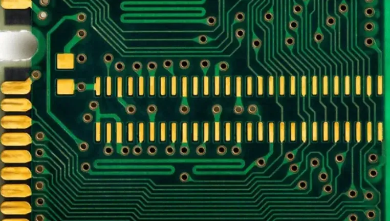
OSP, or Organic Solderability Preservative, is a surface finish applied to the exposed copper traces and pads of a PCB to protect them from oxidation. This thin, organic coating acts as a barrier, preserving the solderability of the copper until the board is ready for component assembly. Unlike metallic finishes like HASL (Hot Air Solder Leveling) or ENIG (Electroless Nickel Immersion Gold), OSP uses a water-based chemical compound, making it a unique and environmentally friendly option.
In the OSP process, a layer of organic material—typically based on azole compounds like benzotriazole or imidazole—is chemically bonded to the copper surface. This layer, often just 0.2 to 0.5 microns thick, ensures that the copper remains clean and solderable for a limited period, usually up to 6-12 months under proper storage conditions.
How Does the OSP Process Work?
The OSP process is relatively simple compared to other surface treatments, which contributes to its cost-effectiveness. Here's a step-by-step breakdown of how OSP is applied during PCB manufacturing:
- Cleaning: The PCB undergoes a thorough cleaning to remove any contaminants, oxides, or residues from the copper surface. This step is crucial to ensure proper adhesion of the OSP coating.
- Micro-Etching: A light etching process creates a slightly rough surface on the copper, enhancing the bonding of the organic compound.
- OSP Application: The board is immersed in a solution containing the organic preservative. The chemical reaction forms a thin, uniform layer over the copper, typically within a few minutes.
- Rinsing and Drying: Excess solution is rinsed off, and the board is dried to complete the process.
The result is a PCB with a nearly invisible coating that protects the copper while maintaining excellent solderability. However, this coating is temporary and can degrade if exposed to harsh conditions or improper handling.
Advantages of OSP in PCB Manufacturing
OSP has gained popularity in the electronics industry due to several key benefits. If you're considering OSP for your PCB projects, here are the main advantages to keep in mind:
- Cost-Effective: The OSP process uses simple chemical compounds and requires less complex equipment compared to metallic finishes. This results in lower production costs, often making OSP one of the most affordable surface treatments available.
- Environmentally Friendly: Since OSP is a water-based process and does not involve heavy metals like lead or nickel, it aligns with green manufacturing standards such as RoHS (Restriction of Hazardous Substances). This makes it a preferred choice for eco-conscious projects.
- Excellent Solderability: OSP provides good wettability, meaning solder flows smoothly over the copper during assembly. This leads to strong, reliable solder joints when flux is applied to vias and pads.
- Simple and Reworkable: The manufacturing process for OSP is straightforward, and if the coating is damaged, it can often be reworked by reapplying the preservative. This flexibility is a significant advantage for manufacturers.
- Flat Surface Finish: Unlike some finishes that create uneven surfaces, OSP results in a flat copper surface, which is ideal for fine-pitch components and high-density designs.
For example, in a consumer electronics project requiring a high-density PCB with a 0.2 mm BGA (Ball Grid Array) spacing, OSP can ensure precise soldering without the risk of uneven surfaces interfering with component placement.
Disadvantages of OSP in PCB Manufacturing
While OSP offers many benefits, it is not without limitations. Understanding these drawbacks will help you decide if OSP is the right choice for your specific application.
- Limited Shelf Life: The organic coating on OSP-treated PCBs is temporary and can degrade over time. If exposed to air for more than 10-15 days or stored improperly, the coating may fail, leading to oxidation of the copper and poor solderability. Under ideal conditions (vacuum-sealed storage at controlled temperature and humidity), shelf life can extend to 6-12 months.
- Sensitivity to Handling: OSP coatings are delicate and can be damaged by fingerprints, moisture, or harsh environmental conditions. This requires careful handling and storage during manufacturing and assembly.
- Not Suitable for Multiple Reflows: OSP is generally not recommended for PCBs that will undergo multiple reflow soldering processes. The organic layer can break down under repeated high-temperature exposure, reducing solderability.
- Limited Durability: Unlike metallic finishes, OSP does not provide long-term protection against corrosion. Once the coating is removed during soldering, the exposed copper is vulnerable to oxidation if not immediately assembled.
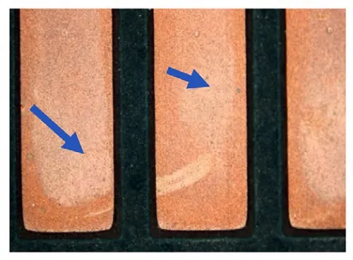
- Inspection Challenges: The nearly invisible OSP coating makes it difficult to visually inspect for coverage or defects. Specialized testing may be required to ensure quality.
For instance, if you're designing a PCB for an industrial application that requires long-term storage before assembly, OSP might not be the best choice due to its limited shelf life.
Applications of OSP in PCB Manufacturing
OSP is widely used across various industries due to its affordability and environmental benefits. Here are some common applications where OSP shines as a PCB surface treatment:
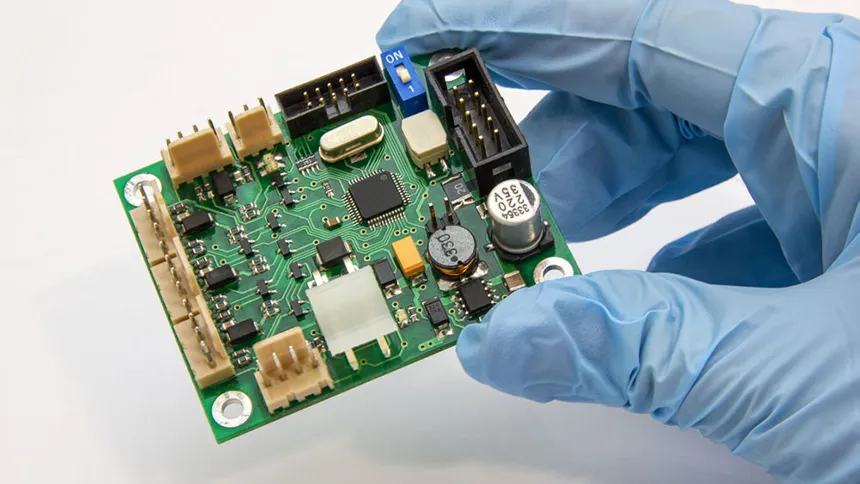
- Consumer Electronics: OSP is frequently used in smartphones, tablets, and other consumer devices where cost savings and compliance with green regulations are priorities. Its flat surface finish also supports the high-density designs typical in these products.
- Automotive Electronics: For non-critical components in automotive systems, OSP provides a budget-friendly option. However, it is less common in harsh environments where durability is critical.
- Industrial Controls: OSP is suitable for PCBs in industrial control systems that are assembled quickly and not exposed to extreme conditions during storage.
- Single-Sided and Double-Sided PCBs: OSP works well for simpler board designs with fewer layers, where complex soldering processes or long-term durability are not major concerns.
It's worth noting that OSP is less ideal for high-reliability applications like aerospace or medical devices, where metallic finishes with greater durability are often preferred. For a typical consumer-grade PCB with a 2-layer design and a line width/spacing of 3 mil/3 mil, OSP can be an excellent fit if assembly happens within the recommended timeframe.
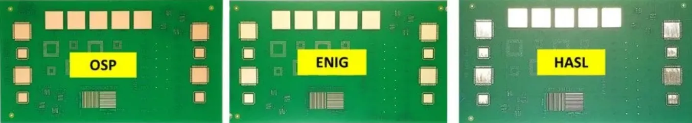
OSP vs. Other PCB Surface Treatments
To better understand where OSP fits in the spectrum of PCB surface treatments, let's compare it to two other common finishes: HASL and ENIG.
- OSP vs. HASL: HASL involves coating the PCB with a layer of solder, resulting in a thicker, more durable finish than OSP. However, HASL can create uneven surfaces, making it less suitable for fine-pitch components. OSP, on the other hand, offers a flatter finish but lacks the durability of HASL for long-term storage or multiple reflows.
- OSP vs. ENIG: ENIG provides a robust, long-lasting finish with excellent corrosion resistance due to its nickel and gold layers. It is ideal for high-reliability applications but comes at a higher cost. OSP is more affordable and eco-friendly but cannot match ENIG's durability or shelf life.
For a project with a tight budget and a quick assembly timeline, OSP often outperforms these alternatives. However, for applications requiring a shelf life beyond 12 months or exposure to harsh conditions, other finishes might be more appropriate.
Best Practices for Using OSP in PCB Manufacturing
To maximize the benefits of OSP and minimize its limitations, follow these practical tips during design, manufacturing, and assembly:
- Proper Storage: Store OSP-treated PCBs in vacuum-sealed packaging with controlled temperature (below 30°C) and humidity (below 60%) to extend shelf life. Avoid exposure to air for more than 10-15 days before assembly.
- Minimize Handling: Use gloves when handling OSP-coated boards to prevent contamination from fingerprints or oils. Train staff on proper handling techniques to avoid damaging the delicate coating.
- Quick Assembly: Plan your manufacturing process to ensure OSP-treated PCBs are assembled as soon as possible after production. Delays can lead to degradation of the coating.
- Single Reflow Process: Design your assembly process to limit OSP-treated PCBs to a single reflow soldering cycle. If multiple reflows are necessary, consider an alternative finish.
- Quality Control: Implement testing methods, such as solderability tests, to verify the integrity of the OSP coating before assembly, as visual inspection alone may not detect defects.
By adhering to these practices, you can ensure reliable performance from OSP-treated PCBs, even with their inherent limitations.
Conclusion: Is OSP Right for Your PCB Project?
OSP (Organic Solderability Preservative) is a versatile and budget-friendly surface treatment for PCB manufacturing, offering excellent solderability, environmental benefits, and a flat finish ideal for high-density designs. However, its limited shelf life, sensitivity to handling, and unsuitability for multiple reflows make it less ideal for certain applications. By understanding the OSP process, its advantages, disadvantages, and best use cases, you can make an informed decision about whether it fits your project needs.
Whether you're working on consumer electronics, automotive components, or industrial controls, OSP can be a valuable choice when cost and eco-friendliness are priorities. With proper handling and timely assembly, OSP delivers reliable results for a wide range of PCB designs. As you plan your next project, weigh the trade-offs of OSP against other surface treatments to ensure optimal performance and durability.
For more insights into PCB surface treatments and manufacturing solutions, explore our resources and stay updated on the latest industry trends. Your next innovative design starts with the right foundation!


