 ALLPCB


Designing a multi-layer PCB stack-up is a critical step in ensuring the performance, reliability, and cost-efficiency of modern electronic devices. Whether you're working on high-speed circuits, compact designs, or complex systems, a well-planned multi-layer PCB stack-up can make all the difference. In this comprehensive guide, we’ll walk you through the essentials of multi-layer PCB stack-up design, covering layer arrangement, material selection, impedance matching, and cost optimization. By the end, you'll have actionable insights to create boards that meet your performance goals.
What Is Multi-Layer PCB Stack-Up Design?
A multi-layer PCB stack-up refers to the arrangement of conductive and insulating layers in a printed circuit board with three or more layers. Unlike single or double-sided boards, multi-layer PCBs allow for higher component density, improved signal integrity, and better power distribution. The stack-up design dictates how these layers are ordered, what materials are used, and how signals and power flow through the board.
Getting the stack-up right is vital for minimizing issues like noise, crosstalk, and signal loss, especially in high-speed applications. With the increasing demand for compact and powerful electronics, understanding multi-layer PCB layer arrangement and related factors is more important than ever.
Why Multi-Layer PCB Stack-Up Design Matters
The design of a multi-layer PCB stack-up directly impacts several key aspects of a circuit board’s performance:
- Signal Integrity: Poor layer arrangement can lead to crosstalk or signal delays, especially in high-speed designs operating at frequencies above 1 GHz.
- Power Distribution: Proper placement of power and ground planes reduces voltage drops and ensures stable operation.
- Thermal Management: The right materials and layer order can help dissipate heat effectively, preventing overheating in dense designs.
- Cost Efficiency: Optimizing the stack-up can reduce manufacturing costs without compromising quality.
With these benefits in mind, let’s dive into the core elements of designing a multi-layer PCB stack-up for optimal performance.
Key Elements of Multi-Layer PCB Stack-Up Design
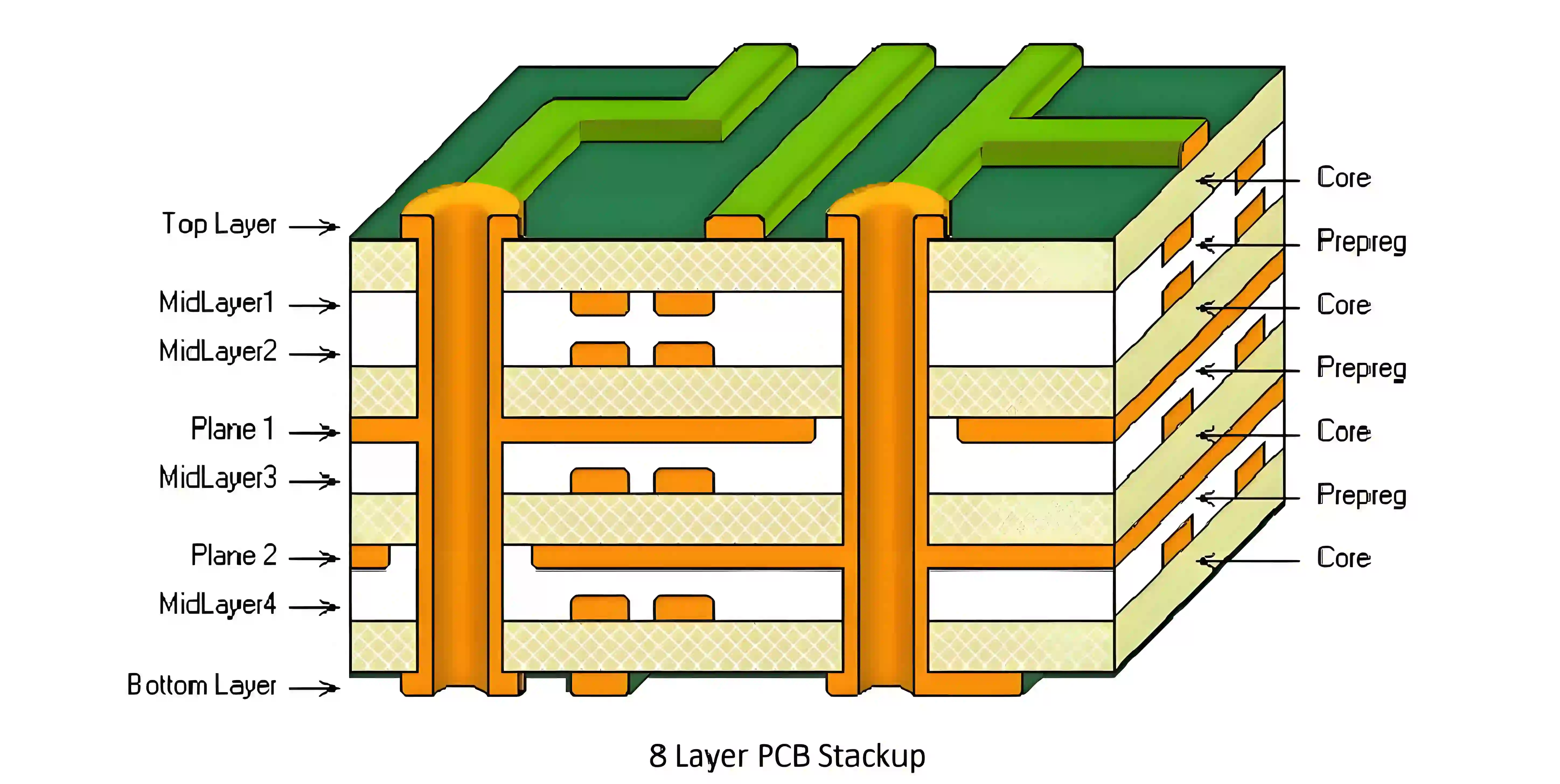
1. Multi-Layer PCB Layer Arrangement
The arrangement of layers in a multi-layer PCB is the foundation of a successful design. A typical stack-up includes signal layers, power planes, and ground planes, each serving a specific purpose. Here’s a breakdown of common practices for arranging layers:
- Signal Layers: These are used for routing traces that carry data or control signals. High-speed signals should be placed on outer layers or near ground planes to minimize interference.
- Ground Planes: These layers provide a low-impedance return path for signals and help reduce electromagnetic interference (EMI). Place ground planes adjacent to signal layers for better shielding.
- Power Planes: These distribute power to components. Positioning power and ground planes next to each other creates a distributed capacitance, improving power delivery.
For a 6-layer PCB, a common stack-up might look like this:
- Top Signal Layer
- Ground Plane
- Signal Layer (Internal)
- Power Plane
- Ground Plane
- Bottom Signal Layer
This setup balances signal integrity and power distribution. For higher layer counts, such as 8 or 12 layers, additional signal and plane layers can be added while maintaining symmetry to avoid warping during manufacturing.
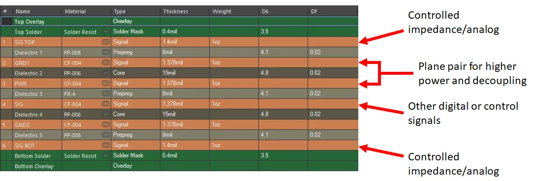
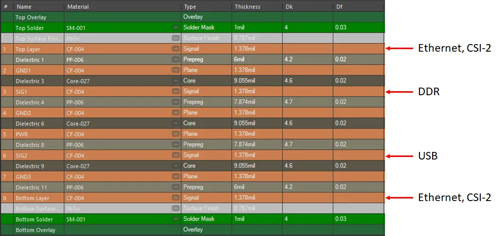
2. Multi-Layer PCB Material Selection
Choosing the right materials for your multi-layer PCB stack-up is just as important as layer arrangement. Materials impact signal speed, thermal performance, and cost. Here are key factors to consider:
- Dielectric Material: The dielectric constant (Dk) of the insulating material affects signal propagation speed. For high-speed designs, materials with a low Dk (e.g., 3.0 to 4.0) like PTFE or advanced laminates are ideal. Standard FR-4, with a Dk of around 4.5, works well for lower-speed applications.
- Loss Tangent (Df): This measures signal loss in the material. Low-loss materials (Df below 0.005) are critical for frequencies above 5 GHz to prevent signal degradation.
- Thermal Conductivity: For designs with high power dissipation, choose materials with better thermal conductivity to manage heat. Some advanced materials can handle temperatures up to 150°C without degrading.
- Thickness: Thinner dielectric layers (e.g., 0.1 mm) are useful for tight impedance control, while thicker layers (e.g., 0.5 mm) provide structural stability.
Balancing performance and cost is key in material selection. High-performance materials often come with a higher price tag, so evaluate your project’s needs carefully.
3. Multi-Layer PCB Impedance Matching
Impedance matching is crucial for maintaining signal integrity in high-speed designs. Mismatched impedance can cause reflections, leading to signal loss or data errors. Here’s how to achieve proper impedance matching in a multi-layer PCB stack-up:
- Controlled Impedance Traces: Design trace widths and spacing based on the target impedance, often 50 ohms for single-ended signals or 100 ohms for differential pairs. Use impedance calculators or simulation tools to determine the correct dimensions.
- Layer Proximity: Place high-speed signal traces close to a reference plane (ground or power) to maintain consistent impedance. A typical separation might be 0.1 mm to 0.2 mm for a 50-ohm trace on standard FR-4 material.
- Dielectric Consistency: Ensure the dielectric material between layers is uniform to avoid impedance variations. Variations as small as 10% can cause significant signal issues at frequencies above 1 GHz.
Simulation software can help predict impedance and identify potential issues before manufacturing. Testing a prototype board with a Time Domain Reflectometer (TDR) can also verify impedance values.
4. Multi-Layer PCB Cost Optimization
While performance is critical, keeping costs under control is equally important. Multi-layer PCB cost optimization involves making smart design choices without sacrificing quality. Consider these strategies:
- Minimize Layer Count: Use the fewest layers necessary to meet design requirements. For example, a 4-layer board is often cheaper than a 6-layer board while still supporting many applications.
- Standard Materials: Opt for widely available materials like FR-4 unless high-speed or thermal performance demands advanced options. This can reduce costs by up to 30% compared to specialty laminates.
- Symmetrical Stack-Up: Design a balanced stack-up to prevent warping, which can lead to manufacturing defects and costly reworks.
- Panel Utilization: Optimize board size and layout to fit multiple units on a single manufacturing panel, reducing waste and lowering per-unit costs.
- Avoid Complex Features: Limit the use of blind or buried vias unless absolutely necessary, as they increase fabrication complexity and cost by 20-50%.
Work closely with your manufacturing partner to understand their capabilities and constraints. This collaboration can help identify cost-saving opportunities early in the design process.
Best Practices for Multi-Layer PCB Stack-Up Design
To achieve optimal performance, follow these best practices when designing your multi-layer PCB stack-up:
- Maintain Symmetry: Keep the stack-up balanced to avoid mechanical stress during manufacturing. For instance, in an 8-layer board, ensure signal and plane layers are mirrored around the center.
- Prioritize Ground Planes: Place ground planes near high-speed signal layers to provide a stable return path and reduce EMI.
- Route High-Speed Signals First: Plan routing for critical signals on outer layers or near reference planes before addressing lower-speed traces.
- Simulate and Test: Use simulation tools to model signal behavior and test prototypes to catch issues like crosstalk or impedance mismatches early.
- Consider Manufacturing Tolerances: Account for variations in material thickness or trace etching, which can affect impedance by up to 5-10%.
Following these guidelines can significantly improve the reliability and performance of your multi-layer PCB designs.
Common Challenges in Multi-Layer PCB Stack-Up Design
Designing a multi-layer PCB stack-up isn’t without its challenges. Here are some common issues and how to address them:
- Crosstalk: This occurs when signals interfere with each other. Minimize it by increasing spacing between traces or adding ground planes between signal layers.
- Thermal Issues: High-density designs can overheat. Use materials with better thermal conductivity and add thermal vias to dissipate heat.
- Signal Delay: Longer traces or improper layer placement can cause delays. Keep critical traces short and route them on layers with minimal dielectric thickness.
- Manufacturing Defects: Misalignment or warping can occur with unbalanced stack-ups. Design with symmetry and consult with manufacturers on their process capabilities.
Being proactive about these challenges during the design phase can save time and resources in the long run.
Tools for Multi-Layer PCB Stack-Up Design
Several tools can assist in designing an effective multi-layer PCB stack-up:
- CAD Software: Use design platforms with built-in layer stack managers to visualize and adjust your stack-up.
- Impedance Calculators: Online tools or integrated features in design software can help calculate trace dimensions for specific impedance values.
- Simulation Tools: Software for electromagnetic simulation can predict signal behavior and identify potential issues before fabrication.
Investing time in learning these tools can streamline the design process and improve outcomes.
Conclusion: Mastering Multi-Layer PCB Stack-Up Design
Designing a multi-layer PCB stack-up for optimal performance requires careful planning and attention to detail. From multi-layer PCB layer arrangement to material selection, impedance matching, and cost optimization, each aspect plays a vital role in the success of your design. By following the strategies and best practices outlined in this guide, you can create boards that meet the demands of modern electronics—whether you're working on high-speed, compact, or power-intensive applications.
At ALLPCB, we’re committed to supporting engineers with the resources and expertise needed to bring their designs to life. With a well-thought-out multi-layer PCB stack-up, you’re one step closer to achieving reliable, high-performing circuit boards that stand out in today’s competitive market.


