 ALLPCB


Are you looking to enhance the durability and reliability of your printed circuit boards (PCBs) with a superior surface finish? Hard gold plating for PCBs is a top choice for applications requiring high wear resistance and excellent conductivity. In this comprehensive guide, we’ll dive deep into everything you need to know about hard gold plating, including its applications, detailed process steps, design considerations, thickness standards, troubleshooting tips, and best practices. Whether you’re an engineer, designer, or manufacturer, this guide will equip you with actionable insights to optimize your PCB projects with hard gold plating.
What Is Hard Gold Plating for PCBs?
Hard gold plating is a surface finish applied to specific areas of a PCB, such as edge connectors or contact points, to provide exceptional durability and resistance to wear. Unlike other gold finishes, hard gold is alloyed with elements like cobalt or nickel to increase its hardness, making it ideal for high-wear applications. This finish ensures reliable electrical connections over thousands of cycles, often exceeding 10,000 mating cycles without significant degradation.
In the following sections, we’ll explore why hard gold plating is a preferred choice, how it’s applied, and how to ensure the best results for your PCB designs.
Key Applications of Hard Gold Plating in PCB Design
Hard gold plating is widely used in industries where reliability and longevity are critical. Here are some primary applications where this finish excels in PCB design:
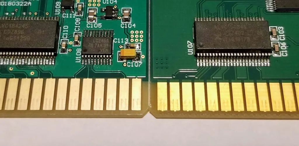
- Edge Connectors: Hard gold is commonly applied to edge connectors (also known as gold fingers) on PCBs used in computers, servers, and industrial equipment. These connectors endure frequent insertion and removal, and hard gold ensures minimal wear, maintaining signal integrity over time.
- Keypads and Membrane Switches: In devices like calculators or industrial control panels, hard gold plating on contact points withstands repeated mechanical stress, ensuring consistent performance.
- High-Reliability Electronics: Aerospace, medical, and military applications often rely on hard gold plating for its corrosion resistance and ability to perform in harsh environments.
- Test Equipment: PCBs in testing and measurement devices benefit from hard gold’s durability, as they often require frequent connections and disconnections.
Understanding Hard Gold Plating Thickness for Optimal Performance
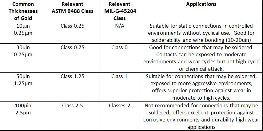
The thickness of hard gold plating plays a crucial role in balancing durability, cost, and performance. Hard gold plating thickness typically ranges from 0.8 to 2.5 microns (30 to 100 microinches), depending on the application and industry standards.
- General Use (30-50 microinches): For applications with moderate wear, such as consumer electronics, a thickness of 0.8 to 1.3 microns is often sufficient. This provides a good balance between cost and durability.
- High-Wear Applications (50-100 microinches): In industrial or military equipment where connectors face thousands of mating cycles, a thicker layer of 1.3 to 2.5 microns is recommended to ensure longevity.
- Cost Considerations: Thicker gold layers increase material costs, so it’s important to specify only the necessary thickness based on the expected wear and environmental conditions.
Adhering to appropriate thickness not only ensures performance but also prevents issues like cracking or poor adhesion. Always consult with your manufacturing partner to determine the ideal thickness for your specific PCB design needs.
Hard Gold Plating Process Steps: A Step-by-Step Overview
The hard gold plating process for PCBs involves several meticulous steps to ensure a uniform, durable finish. Understanding these steps can help in optimizing your design and avoiding common pitfalls. Below is a detailed breakdown of the hard gold plating process steps:
- Surface Preparation: The PCB surface, typically copper, is thoroughly cleaned to remove contaminants like oils, oxides, or residues. This step often involves chemical cleaning or micro-etching to ensure proper adhesion of subsequent layers.
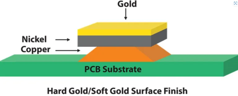
- Nickel Underplating: A layer of nickel, usually 3 to 6 microns thick, is electroplated onto the copper surface. This acts as a barrier layer to prevent diffusion between copper and gold, enhancing durability and corrosion resistance.
- Hard Gold Deposition: The hard gold layer is then electroplated over the nickel. The gold is alloyed with small amounts of cobalt or nickel (typically 0.1-0.3%) to increase hardness. The plating bath is carefully controlled for temperature, current density, and composition to achieve uniform thickness, often between 0.8 and 2.5 microns.
- Post-Plating Inspection: After plating, the PCB undergoes inspection for thickness, adhesion, and surface quality using tools like X-ray fluorescence (XRF) for precise measurement of gold thickness.
- Final Cleaning and Protection: Any residues from the plating process are removed, and the board is prepared for further assembly or packaging, ensuring the gold surface remains uncontaminated.
Each step requires precision to avoid defects like uneven plating or poor adhesion, which can compromise the PCB’s performance. Working with an experienced manufacturer ensures these steps are executed flawlessly.
Hard Gold Plating Standards: Ensuring Quality and Compliance
Compliance with industry standards is essential for producing reliable PCBs with hard gold plating. These standards define acceptable thickness, adhesion, and wear resistance to ensure consistent quality. Some widely recognized hard gold plating standards include:
- IPC-6012: This standard covers the qualification and performance of rigid PCBs, including specifications for hard gold plating thickness and durability. It often specifies a minimum thickness of 0.8 microns for general applications and up to 2.5 microns for high-wear areas.
- IPC-4552: Focused on electroless nickel/immersion gold (ENIG) and hard gold finishes, this standard provides guidelines for plating quality, including adhesion tests and solderability requirements.
- MIL-G-45204: A military standard often referenced for hard gold plating, specifying gold purity (minimum 99.7%) and hardness (130-200 Knoop Hardness Number) to meet rigorous performance criteria.
Ensuring your PCB design and manufacturing process align with these standards guarantees reliability, especially for critical applications in aerospace or medical fields. Always verify that your manufacturing partner adheres to these guidelines.
Hard Gold Plating Troubleshooting: Common Issues and Solutions
Even with a well-defined process, issues can arise during hard gold plating that affect the PCB’s performance. Here are some common hard gold plating troubleshooting tips to address potential problems:
- Uneven Thickness: If the gold layer varies in thickness across the PCB, it may result from inconsistent current distribution during plating. Ensure the plating bath is properly agitated and that the current density (typically 1-5 ASF, or amperes per square foot) is optimized for uniform deposition.
- Poor Adhesion: Gold peeling or flaking often indicates inadequate surface preparation or a defective nickel underlayer. Double-check the cleaning process and verify the nickel layer’s integrity (3-6 microns thick) before gold plating.
- Discoloration or Tarnishing: This can occur due to contamination in the plating bath or exposure to harsh environments post-plating. Maintain strict control over bath chemistry and store finished PCBs in a clean, dry environment.
- Excessive Wear: If the gold wears out prematurely, the thickness may be insufficient for the application. Review the mating cycle requirements and consider increasing the gold thickness to 1.3-2.5 microns for high-wear areas.
Proactive monitoring during the manufacturing process can prevent many of these issues. Regular testing for thickness and adhesion, using tools like XRF or cross-sectional analysis, can catch problems early.
Best Practices for Hard Gold Plating in PCB Design
To achieve optimal results with hard gold plating in PCB design, follow these best practices tailored for engineers and designers:
- Specify Plating Areas Clearly: Use design files to indicate exactly where hard gold plating is needed, such as on edge connectors or specific pads. Avoid unnecessary plating to reduce costs, as gold is expensive compared to other finishes.
- Choose the Right Thickness: Match the gold thickness to the application’s wear and environmental requirements. For instance, use 0.8-1.3 microns for moderate wear and up to 2.5 microns for high-cycle applications.
- Ensure Proper Nickel Underlayer: A uniform nickel layer of 3-6 microns is critical for adhesion and durability. Specify this in your design requirements to avoid issues like gold peeling.
- Collaborate with Manufacturers Early: Work closely with your PCB fabrication partner during the design phase to confirm that your hard gold plating requirements are feasible and cost-effective.
- Test for Reliability: After production, conduct wear tests (e.g., mating cycle tests up to 10,000 cycles) and environmental testing (e.g., salt spray tests for corrosion resistance) to validate the plating’s performance.
Implementing these practices not only enhances the quality of your PCBs but also minimizes costly rework or failures in the field.
Advantages and Limitations of Hard Gold Plating for PCBs
Understanding the pros and cons of hard gold plating helps in deciding if it’s the right finish for your PCB project.
Advantages
- High Durability: Hard gold withstands thousands of mating cycles (often over 10,000), making it ideal for connectors and switches.
- Corrosion Resistance: It offers excellent protection against oxidation and harsh environments, ensuring long-term reliability.
- Superior Conductivity: Gold provides low contact resistance, maintaining signal integrity in high-frequency applications.
Limitations
- Higher Cost: Hard gold plating is more expensive than alternatives like immersion gold or HASL due to material and process costs.
- Limited Solderability: Hard gold is not ideal for soldering as it can lead to brittle joints. It’s typically used only on non-solderable areas like connectors.
- Selective Application: It’s often applied only to specific areas, requiring precise masking during manufacturing, which adds complexity.
Weighing these factors against your project’s requirements will guide you in choosing the most suitable surface finish.
Conclusion: Mastering Hard Gold Plating for PCB Success
Hard gold plating is a powerful solution for enhancing the durability and reliability of PCBs in demanding applications. From edge connectors in servers to contact points in medical devices, this finish ensures long-lasting performance under high wear and harsh conditions. By understanding key aspects like hard gold plating thickness, process steps, standards, and troubleshooting techniques, you can optimize your PCB designs for success.
Remember to follow best practices in design and manufacturing, such as specifying plating areas accurately and collaborating with experienced fabrication partners. With the insights provided in this guide, you’re well-equipped to leverage hard gold plating for superior PCB performance in your next project.


