 ALLPCB


If you're wondering how via-in-pad affects PCB manufacturing costs, the short answer is that it can significantly increase expenses due to additional processes like via filling and the complexity of high-density interconnect (HDI) designs. However, it also offers benefits like improved performance and space efficiency, which can justify the cost in certain applications. In this detailed blog, we’ll break down the factors driving these costs, including via filling cost, HDI PCB cost, and overall PCB manufacturing cost, to give you a clear cost analysis of via-in-pad technology.
What is Via-in-Pad and Why Does It Matter?
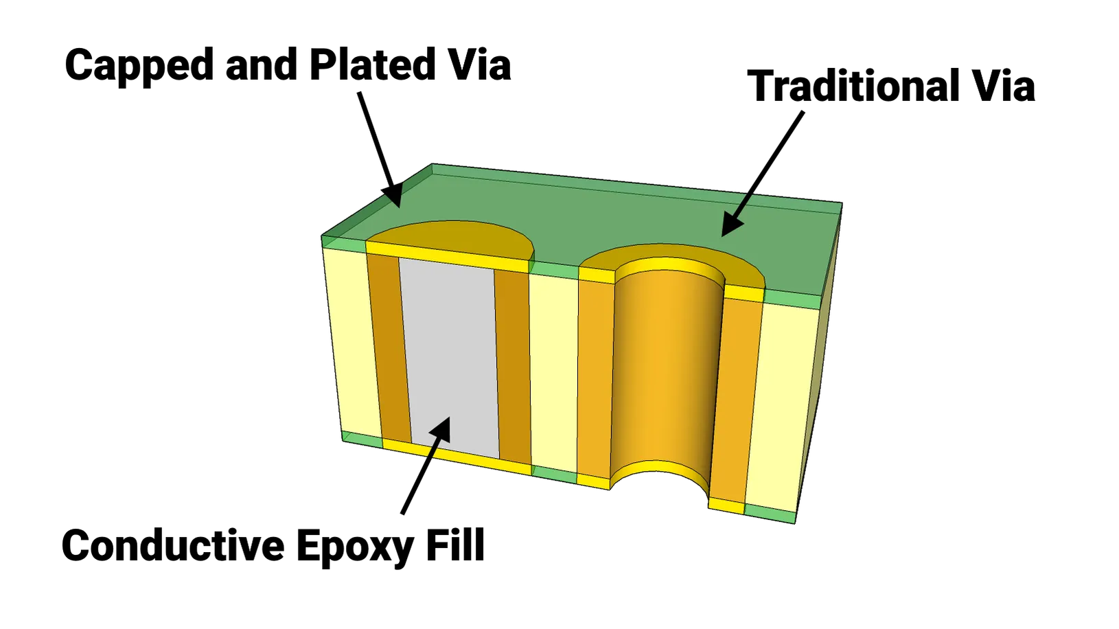
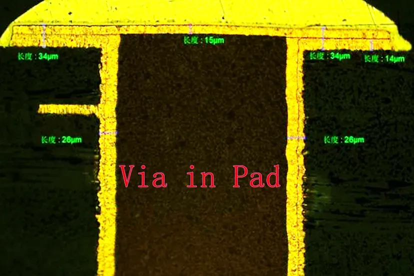
Via-in-pad is a PCB design technique where a via—a small hole that connects different layers of a circuit board—is placed directly within a component’s pad. Unlike traditional vias, which are positioned outside the pad area, this method saves space on the board, making it ideal for compact, high-density designs. It’s commonly used in modern electronics like smartphones, tablets, and other devices where space is at a premium.
While via-in-pad offers advantages like better signal integrity and reduced board size, it comes with a catch: higher manufacturing costs. These costs stem from the specialized processes required to implement this technology, such as via filling and the use of advanced HDI techniques. Understanding these cost factors is crucial for engineers and designers balancing performance with budget constraints.
How Via-in-Pad Impacts PCB Manufacturing Costs
The use of via-in-pad technology directly influences PCB manufacturing costs in several ways. Below, we’ll explore the key factors contributing to the increased expenses, focusing on via filling cost, HDI PCB cost, and other related aspects of cost analysis for via-in-pad.
1. Via Filling Cost: A Necessary Expense
One of the primary reasons via-in-pad increases manufacturing costs is the need for via filling. When a via is placed in a pad, it can create issues during soldering, such as solder wicking into the via, which leads to poor connections. To prevent this, manufacturers fill the via with a conductive or non-conductive material, a process that adds both time and expense.
Conductive filling, often done with copper, improves electrical and thermal performance but is more expensive due to the materials and precision required. Non-conductive filling, typically using epoxy, is cheaper but still adds to the cost compared to unfilled vias. Depending on the board’s requirements, via filling can add anywhere from 10% to 30% to the overall manufacturing cost of a PCB with via-in-pad designs.
For example, in a high-performance board with hundreds of vias, the cost of filling each via might range from $0.01 to $0.05 per via, depending on the material and process used. While this may seem small, it quickly adds up in large-scale production.
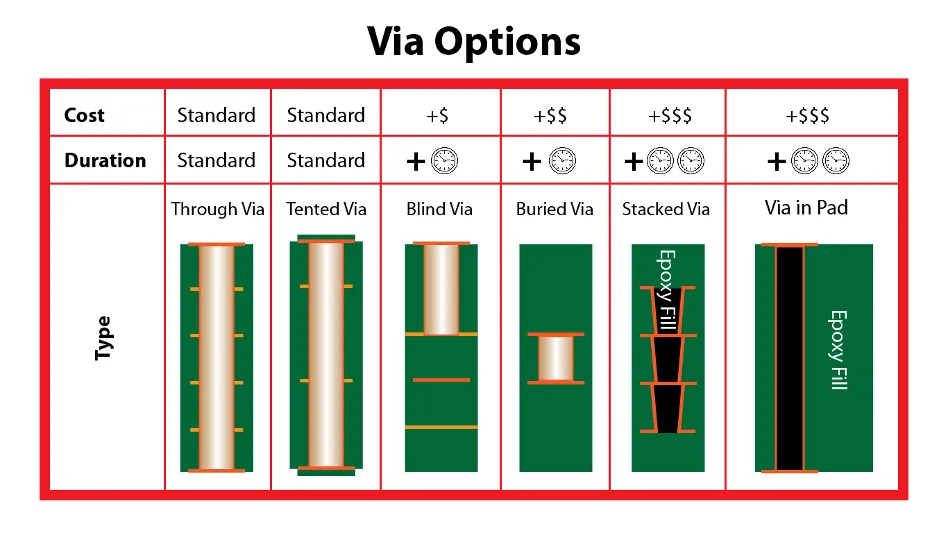
2. HDI PCB Cost: Complexity Drives Up Expenses
Via-in-pad is often used in high-density interconnect (HDI) PCBs, which are designed for compact, multilayer boards with fine traces and small vias. HDI technology itself is more expensive than standard PCB manufacturing due to the advanced equipment, tighter tolerances, and additional layers involved. When via-in-pad is incorporated into an HDI design, the cost rises further because of the precision needed to align vias within pads and the extra steps like laser drilling for microvias.
On average, HDI PCBs can cost 2 to 5 times more than standard multilayer boards. For instance, a standard 4-layer PCB might cost $0.50 per square inch, while an HDI board with via-in-pad could cost $1.50 to $3.00 per square inch, depending on the complexity. This significant jump in HDI PCB cost is a major consideration for projects using via-in-pad technology.
3. Increased Design and Fabrication Complexity
Beyond via filling and HDI requirements, via-in-pad adds complexity to both the design and fabrication phases, further impacting PCB manufacturing cost. Designers must account for tighter spacing, precise via placement, and potential signal integrity issues, which often require advanced software and skilled engineers. These factors can increase design time and labor costs by 15% to 25% compared to traditional PCB layouts.
During fabrication, manufacturers need specialized equipment to handle the small tolerances of via-in-pad designs. For example, laser drilling for microvias (common in via-in-pad) is more costly than mechanical drilling, often adding $0.10 to $0.20 per via. Additionally, the risk of defects is higher, as misaligned vias or improper filling can lead to board failures, increasing scrap rates and overall production costs.
Cost Analysis of Via-in-Pad: Weighing the Pros and Cons
While the costs associated with via-in-pad are clear, it’s important to perform a thorough cost analysis to determine whether the benefits outweigh the expenses for your specific project. Let’s look at the advantages and trade-offs to help you make an informed decision.
Benefits of Via-in-Pad That May Justify the Cost
- Space Savings: By placing vias directly in pads, you can reduce the overall size of the PCB, which is critical for compact devices. This can lower material costs in some cases, though it’s often offset by higher fabrication expenses.
- Improved Signal Integrity: Via-in-pad reduces the length of signal paths, minimizing impedance mismatches. For high-speed designs operating at frequencies above 1 GHz, this can improve performance significantly, potentially reducing the need for costly redesigns.
- Better Thermal Management: Conductive via filling enhances heat dissipation, which is vital for components like power ICs that generate significant heat. This can extend the lifespan of the device, saving on long-term maintenance costs.
Drawbacks and Cost Considerations
- Higher Upfront Costs: As discussed, via filling cost and HDI PCB cost drive up the initial investment. For low-volume production, these costs may not be justifiable.
- Manufacturing Challenges: The risk of defects and the need for specialized processes can lead to higher rejection rates, increasing waste and overall PCB manufacturing cost.
- Limited Manufacturer Options: Not all PCB fabricators have the capability to handle via-in-pad designs, especially with HDI. This can limit your choices and potentially lead to higher pricing due to reduced competition.
Strategies to Manage Via-in-Pad Costs
While via-in-pad inherently increases PCB manufacturing costs, there are ways to mitigate these expenses without sacrificing performance. Here are some practical tips for engineers and designers:
- Optimize Via Placement: Use via-in-pad only where necessary, such as for high-speed signals or space-constrained areas. For less critical components, stick to traditional vias to reduce via filling costs.
- Choose Cost-Effective Filling Materials: If thermal or electrical performance isn’t a priority, opt for non-conductive epoxy filling over copper to save on material costs.
- Work with Experienced Manufacturers: Partner with a fabricator skilled in HDI and via-in-pad processes to minimize defects and rework, which can lower overall PCB manufacturing cost.
- Balance HDI Complexity: Avoid over-specifying the number of layers or microvias in HDI designs. Simplifying the board where possible can reduce HDI PCB cost significantly.
Real-World Applications and Cost Implications
Understanding how via-in-pad impacts costs becomes even clearer when looking at real-world applications. For instance, in the smartphone industry, where board space is extremely limited, via-in-pad is often used to fit more components into a smaller area. While the upfront cost might be 20% higher than a traditional design, the ability to create a thinner, lighter device can lead to greater market competitiveness and higher sales, offsetting the initial expense.
In contrast, for industrial control systems where space isn’t as critical, the added cost of via-in-pad might not be worth it. A standard multilayer board with traditional vias could achieve the same functionality at a lower cost, making it a more economical choice.
Conclusion: Is Via-in-Pad Worth the Cost?
Via-in-pad technology undoubtedly increases PCB manufacturing costs due to factors like via filling cost, HDI PCB cost, and fabrication complexity. However, the benefits—such as space savings, improved signal integrity, and better thermal management—can make it a worthwhile investment for high-performance, compact designs. By conducting a detailed cost analysis of via-in-pad for your specific project and applying cost-saving strategies, you can strike a balance between budget and performance.


