 ALLPCB


As a PCB manufacturer, we often encounter designs where thickness tolerance is overlooked, leading to unexpected challenges. Ignoring PCB thickness tolerance can result in significant cost implications, reduced yield, increased material waste, and manufacturing delays. In this blog, we’ll dive deep into how PCB thickness tolerance impacts your project and why paying attention to tight tolerance in PCB manufacturing is critical for success.
From performance issues to production inefficiencies, the hidden costs of neglecting this crucial specification can spiral out of control. Let’s explore the real-world effects of PCB thickness tolerance on cost, yield, and waste, and share actionable insights to help you avoid these pitfalls.
What Is PCB Thickness Tolerance and Why Does It Matter?
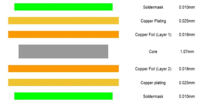
PCB thickness tolerance refers to the allowable variation in the thickness of a printed circuit board during manufacturing. Standard PCB thicknesses typically range from 0.4mm to 3.2mm, with tolerances often specified as ±10% or tighter, depending on the application. For example, a 1.6mm board with a ±10% tolerance can vary between 1.44mm and 1.76mm.
This variation might seem minor, but it plays a huge role in the board’s performance and manufacturability. Thickness affects impedance control, signal integrity, and mechanical fit in enclosures. When tolerance is ignored, the risks include electrical failures, assembly issues, and even complete redesigns—each adding to project costs.
In high-frequency applications, for instance, a deviation in thickness can alter the dielectric constant, impacting signal speeds. A typical FR-4 material at 1.6mm thickness might have a dielectric constant of 4.5, but a 0.2mm deviation could shift impedance by several ohms, disrupting performance. Tight tolerance PCB manufacturing ensures these variations are minimized, but it comes at a price—one that’s often worth paying when compared to the hidden costs of neglect.
PCB Thickness Tolerance Cost Implications: The Financial Burden
The cost implications of ignoring PCB thickness tolerance are often underestimated. When boards fall outside the specified tolerance range, manufacturers face several financial hurdles:
- Rejection and Rework Costs: If a batch of boards doesn’t meet thickness specs, they may be rejected during quality control. Reworking or scrapping these boards means additional labor and material expenses. For instance, producing a small run of 100 boards might cost $500, but scrapping half due to tolerance issues doubles your effective cost per usable board.
- Delays in Production: Non-conforming boards can halt assembly lines, delaying delivery schedules. Late deliveries may incur penalties or lost business opportunities, especially in industries like automotive or aerospace where timelines are strict.
- Tooling and Setup Adjustments: Tight tolerance PCB manufacturing often requires specialized tooling or process adjustments. If tolerances are ignored early on, retrofitting production setups mid-process can add hundreds or thousands of dollars to the project.
These costs compound quickly. A project initially budgeted at $10,000 can balloon to $15,000 or more when rework and delays are factored in. Specifying and adhering to realistic thickness tolerances from the design stage can prevent these unexpected expenses.
PCB Thickness Tolerance Impact on Yield: Why Fewer Boards Pass Inspection
Yield—the percentage of usable boards from a production run—is directly tied to how well thickness tolerances are controlled. When tolerances are too loose or ignored, the impact on yield can be severe:
- Inconsistent Electrical Performance: In high-speed designs, even a 0.1mm deviation in thickness can cause impedance mismatches. For a 50-ohm trace, a thickness variation might shift impedance to 55 ohms or higher, leading to signal reflections and failures. Boards failing electrical tests are scrapped, lowering yield.
- Mechanical Fit Issues: Boards that are too thick or thin may not fit into enclosures or connectors. For example, a board designed for a 1.6mm slot but manufactured at 1.8mm could be unusable, reducing the number of passing units.
- Quality Control Failures: During inspection, boards outside tolerance specs are rejected. A typical yield for standard manufacturing might be 95%, but ignoring thickness tolerance can drop this to 80% or lower, meaning more boards are wasted.
Lower yield translates to higher per-unit costs since fewer boards make it to the final product stage. For a run of 1,000 boards, a 15% yield drop means 150 fewer usable units, forcing additional production runs to meet demand—an expensive fix.
PCB Thickness Tolerance and Material Waste: The Environmental and Cost Impact
Material waste is another hidden cost tied to PCB thickness tolerance issues. When boards are manufactured outside the acceptable tolerance range, they’re often scrapped, leading to wasted raw materials and higher environmental impact:
- Scrapped Boards: Each rejected board represents wasted copper, laminate, and other materials. For a standard 1.6mm FR-4 board, the material cost might be $2 per unit, but scrapping 500 boards in a run means $1,000 in direct material loss.
- Energy and Resource Consumption: Manufacturing processes like etching, lamination, and drilling consume energy. When boards are scrapped, this energy is wasted, increasing the carbon footprint of the project.
- Recycling Challenges: While some materials can be recycled, the process isn’t always cost-effective. Disposing of non-recyclable waste adds further costs and environmental strain.
By focusing on tight tolerance PCB manufacturing, waste can be minimized. For example, investing in precise lamination processes might increase upfront costs by 10%, but it can reduce material waste by 20%, offering long-term savings and sustainability benefits.

Suggested Reading: FR-4 vs. Alternatives: How Material Selection Impacts PCB Thickness Tolerance
Tight Tolerance PCB Manufacturing: Balancing Cost and Quality
Tight tolerance PCB manufacturing is the practice of adhering to stricter-than-standard thickness variations, often as low as ±5% or less. While this approach increases production costs, it offers significant benefits that often outweigh the initial investment:
- Improved Performance: For applications like RF or high-speed digital circuits, tight tolerances ensure consistent impedance and signal integrity. A board with a controlled thickness of 1.6mm ±0.05mm can maintain a 50-ohm impedance within 1-2 ohms, reducing signal loss.
- Higher Yield Rates: With tighter control, fewer boards fail inspection, boosting yield. A production run with tight tolerances might achieve a 98% yield compared to 85% for looser specs.
- Reduced Long-Term Costs: While tight tolerance manufacturing may add 15-20% to initial costs, it minimizes rework, waste, and delays, saving money over the project lifecycle.
However, not every project needs tight tolerances. For low-cost, non-critical applications, standard tolerances of ±10% might suffice. The key is to align tolerance specs with the project’s requirements during the design phase to avoid over- or under-specifying.
How to Avoid the Hidden Costs of PCB Thickness Tolerance Issues
Preventing the hidden costs associated with PCB thickness tolerance starts with proactive steps during PCB design and manufacturing. Here are practical tips to ensure your project stays on track:
- Define Clear Specifications: Specify thickness tolerances in your design files. For critical applications, opt for tighter tolerances like ±5% and communicate these needs clearly to your manufacturing partner.
- Collaborate Early: Work with your manufacturer during the design phase to understand their capabilities and limitations. Early collaboration can help identify potential tolerance challenges before production begins.
- Use Quality Materials: Invest in high-quality laminates with consistent thickness properties. Variations in raw materials can lead to tolerance deviations, so choose reliable suppliers.
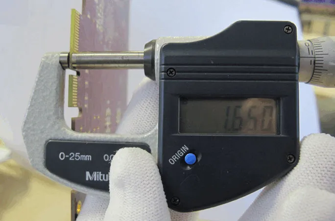
- Implement Strict Quality Control: Ensure that thickness is measured and verified at multiple stages of production. Advanced measurement tools like micrometers or laser scanners can catch deviations early.
- Test Prototypes: Before full-scale production, build and test prototypes to confirm that thickness tolerances meet performance and fit requirements. This step can save thousands in rework costs.
By taking these measures, you can minimize the risks of tolerance-related issues, ensuring smoother production and better cost efficiency.
Real-World Examples: The Consequences of Ignoring Tolerance
Consider a case where a company designed a high-frequency board for a telecommunications device. The design called for a 1.6mm thickness, but tolerance wasn’t specified. During production, boards varied between 1.5mm and 1.7mm, causing impedance mismatches. Signal integrity tests showed a 10% failure rate, leading to a 30% yield drop and $20,000 in rework costs for a 5,000-unit run.
In another instance, a consumer electronics firm ignored thickness tolerance for a low-cost product. The boards, meant to fit into a tight enclosure, were produced at 1.8mm instead of the specified 1.6mm. Over 40% of the batch was unusable, resulting in $15,000 in material waste and delayed product launches.
These examples highlight how seemingly small oversights in thickness tolerance can lead to significant financial and operational setbacks. Tight tolerance PCB manufacturing, while more expensive upfront, could have prevented these issues.
Conclusion: Prioritize PCB Thickness Tolerance for Long-Term Success
Ignoring PCB thickness tolerance can lead to hidden costs that impact your bottom line, from reduced yield and material waste to production delays and rework expenses. As a manufacturer, we’ve seen firsthand how these issues can derail projects, especially in industries where precision is non-negotiable.
By understanding the cost implications of PCB thickness tolerance, its impact on yield, and its role in material waste, you can make informed decisions during design and production. Investing in tight tolerance PCB manufacturing may seem costly at first, but it pays off through higher quality, fewer failures, and long-term savings.
Take the time to define clear specifications, collaborate with your manufacturing partner, and prioritize quality control. These steps will help you avoid the pitfalls of tolerance issues and ensure your PCB projects are successful from start to finish.


