 ALLPCB


In the fast-evolving world of electronics, the demand for more efficient, reliable, and innovative solutions is ever-growing. One of the most exciting advancements in this field is the development of smart PCB panels with embedded sensors. These cutting-edge technologies are transforming the way printed circuit boards (PCBs) are designed, manufactured, and monitored. But what exactly are smart PCB panels, and how do embedded sensors play a role in shaping the future of PCB panelization? In this blog, we’ll dive deep into the concept of smart PCB panels, explore the integration of embedded sensors in PCB manufacturing, and discuss the impact of real-time PCB process monitoring and IoT in PCB manufacturing. Let’s explore how advanced PCB fabrication techniques are paving the way for smarter, more efficient electronics production.
What Are Smart PCB Panels?
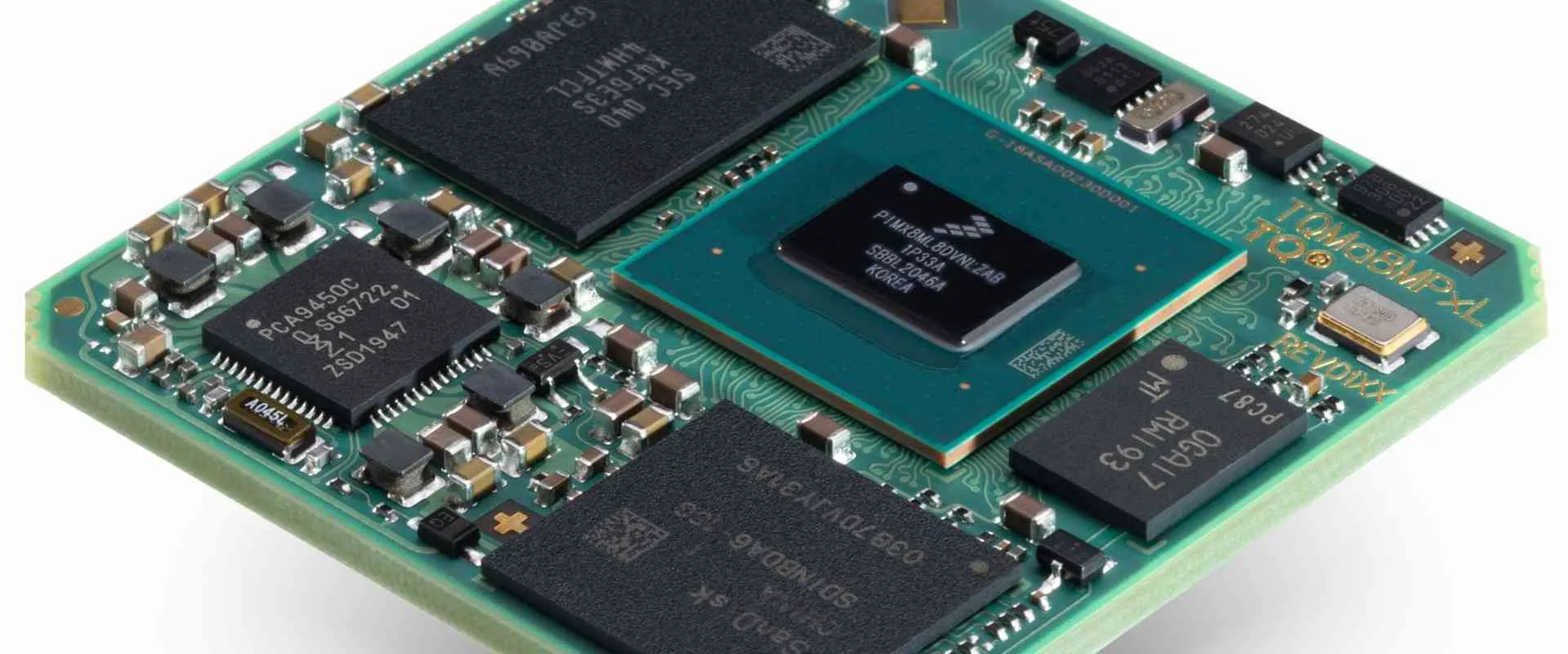
Smart PCB panels are the next generation of printed circuit board technology, designed to go beyond traditional functionality. Unlike conventional PCB panels, which are primarily passive carriers for electronic components, smart panels are equipped with embedded sensors and intelligent features. These sensors can monitor various parameters like temperature, humidity, vibration, and even electrical performance during the manufacturing process and throughout the lifecycle of the board.
The goal of smart PCB panels is to enhance efficiency, improve quality control, and reduce errors in production. By embedding sensors directly into the panel, manufacturers can gather real-time data, enabling proactive decision-making and minimizing costly defects. This innovation is a game-changer for industries that rely on high-precision electronics, such as aerospace, automotive, and medical devices.
The Role of Embedded Sensors in PCB Manufacturing
Embedded sensors in PCB manufacturing are tiny devices integrated directly into the board or panel during the fabrication process. These sensors can detect and measure specific conditions, providing valuable insights into the board’s performance and the manufacturing environment. Let’s break down how these sensors are revolutionizing the industry:
- Quality Assurance: Sensors can detect anomalies like cracks, delamination, or uneven soldering by monitoring stress and strain levels. For instance, a strain sensor might detect a stress value exceeding 500 microstrains, indicating a potential structural issue in the PCB.
- Thermal Management: Temperature sensors embedded in the panel can monitor heat dissipation, ensuring that components operate within safe limits. If a sensor records a temperature above 85°C, it can trigger an alert for cooling adjustments.
- Environmental Monitoring: Humidity sensors can track moisture levels during production, preventing corrosion or material degradation. A humidity reading above 60% could signal the need for environmental controls.
By integrating these sensors, manufacturers can achieve a higher level of precision and reliability. This is especially critical for high-density interconnect (HDI) boards, where even a small defect can lead to significant performance issues.
Real-Time PCB Process Monitoring: A Game-Changer
One of the most significant advantages of smart PCB panels is their ability to enable real-time PCB process monitoring. In traditional manufacturing, quality checks are often performed after key production stages, which means defects might only be detected after considerable time and resources have been invested. With embedded sensors, manufacturers can monitor every step of the process as it happens.
For example, during the soldering phase, sensors can measure the thermal profile to ensure that solder joints are formed correctly. If the temperature deviates from the optimal range of 240-260°C for lead-free soldering, the system can immediately flag the issue. This real-time feedback loop helps reduce scrap rates and ensures that only high-quality boards move forward in production.
Moreover, real-time monitoring extends beyond the factory floor. Once the PCB is deployed in a device, embedded sensors can continue to track performance metrics, providing data on signal integrity (e.g., maintaining impedance values around 50 ohms for high-speed signals) and identifying potential failures before they occur. This predictive maintenance capability is invaluable for industries where downtime is costly.
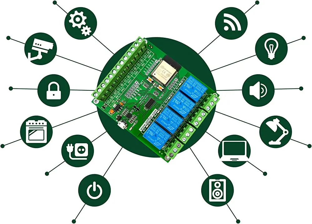
IoT in PCB Manufacturing: Connecting the Dots
The integration of the Internet of Things (IoT) in PCB manufacturing is a natural progression of smart panel technology. IoT refers to the network of connected devices that communicate and share data over the internet. When applied to PCB production, IoT enables seamless connectivity between smart panels, manufacturing equipment, and data analytics platforms.
With IoT, data collected from embedded sensors in smart PCB panels can be transmitted to a centralized system for analysis. For instance, if a vibration sensor detects excessive movement (say, above 5G of force) during the assembly process, the IoT system can alert operators and automatically adjust machinery settings to prevent damage. This level of automation and connectivity is a cornerstone of Industry 4.0, the fourth industrial revolution focused on smart manufacturing.
Additionally, IoT in PCB manufacturing supports traceability. Each panel can be assigned a unique digital identifier, allowing manufacturers to track its journey from raw materials to finished product. This is particularly useful for compliance in regulated industries, ensuring that every board meets stringent standards.
Advanced PCB Fabrication Techniques Behind Smart Panels
The rise of smart PCB panels wouldn’t be possible without advancements in PCB fabrication techniques. These innovative methods allow for the seamless integration of sensors and other smart features without compromising the board’s performance or reliability. Here are some key techniques driving this transformation:
- Additive Manufacturing: Unlike traditional subtractive methods that remove material to create circuits, additive manufacturing builds layers of conductive and insulating materials. This technique allows for precise placement of embedded sensors within the PCB structure.
- Microvia Technology: Microvias are tiny holes drilled into PCBs to connect different layers. Advanced laser drilling techniques create microvias with diameters as small as 50 micrometers, enabling compact designs that can accommodate embedded sensors without increasing board size.
- Flexible and Rigid-Flex PCBs: These boards combine flexibility with durability, making them ideal for integrating sensors in applications where space is limited or movement is frequent. For example, a flexible PCB in a wearable device can house a temperature sensor to monitor skin contact without sacrificing comfort.
These advanced PCB fabrication techniques not only support the integration of smart features but also improve overall board performance. For instance, finer trace widths (down to 3 mils) and tighter spacing (also 3 mils) enable higher signal speeds, crucial for modern high-frequency applications.
Benefits of Smart PCB Panels for Manufacturers and End-Users
The adoption of smart PCB panels with embedded sensors offers a wide range of benefits for both manufacturers and end-users. Let’s explore some of the most impactful advantages:
- Reduced Production Costs: Real-time monitoring and early defect detection lower the likelihood of producing faulty boards, saving on rework and material waste. Studies suggest that implementing smart monitoring can reduce scrap rates by up to 30%.
- Improved Product Reliability: Continuous data collection ensures that PCBs meet performance standards throughout their lifecycle, reducing failure rates in critical applications like medical equipment or automotive systems.
- Faster Time-to-Market: Automated processes driven by IoT and real-time data allow manufacturers to streamline production, cutting down lead times and accelerating product launches.
- Enhanced User Experience: For end-users, smart PCBs mean more reliable devices with features like predictive maintenance, ensuring longer product lifespans and fewer disruptions.
These benefits make smart PCB panels a compelling choice for industries looking to stay competitive in a technology-driven market.
Challenges and Future Outlook for Smart PCB Panels
While the potential of smart PCB panels is immense, there are challenges to overcome. Integrating sensors without increasing production costs significantly is a key concern. Additionally, ensuring data security in IoT-connected systems is critical, as cyber threats could compromise sensitive manufacturing data.
However, ongoing research and development are addressing these hurdles. Innovations in low-cost sensor technology and secure IoT protocols are making smart panels more accessible. Looking ahead, we can expect even smarter PCBs with self-diagnostic capabilities, where boards can not only detect issues but also suggest corrective actions through AI integration.
The future of PCB panelization is undoubtedly tied to smart technology. As industries continue to demand smaller, faster, and more reliable electronics, the role of embedded sensors, real-time monitoring, and IoT in PCB manufacturing will only grow. Manufacturers who embrace these advanced PCB fabrication techniques will be well-positioned to lead in this dynamic landscape.
Conclusion: Embracing the Smart Revolution in PCB Panelization
Smart PCB panels with embedded sensors represent a bold step forward in the world of electronics manufacturing. By leveraging real-time PCB process monitoring, IoT in PCB manufacturing, and advanced PCB fabrication techniques, these panels are setting new standards for quality, efficiency, and innovation. For manufacturers, the benefits of reduced costs, improved reliability, and faster production are clear. For end-users, smarter PCBs mean better-performing, longer-lasting devices.
As technology continues to advance, staying ahead of the curve with smart panel solutions will be essential for success. Whether you’re designing cutting-edge consumer electronics or critical industrial systems, the future of PCB panelization is here—and it’s smarter than ever.


