 ALLPCB


Designing a double-layer PCB can be a balancing act between functionality, cost, and performance. One of the biggest challenges is managing electromagnetic interference (EMI) through effective trace routing. In this comprehensive guide, we’ll explore the art of double-layer PCB trace routing, focusing on strategies to minimize EMI. We’ll dive into key concepts like PCB trace impedance, EMI reduction on PCBs, and the role of a well-designed PCB ground plane. Whether you're an experienced engineer or just starting out, this post will provide actionable tips to enhance your designs.
Why Trace Routing Matters on Double-Layer PCBs
Double-layer PCBs are widely used due to their balance of simplicity and functionality. With only two copper layers, they are more affordable than multi-layer boards while still supporting moderately complex circuits. However, limited space for traces and grounding makes EMI a significant concern. Poor trace routing can lead to signal crosstalk, noise, and interference, which can degrade performance or even cause system failure.
Effective trace routing ensures signals travel with minimal disruption, maintaining signal integrity and reducing EMI. By carefully planning trace paths, controlling impedance, and leveraging a solid ground plane, you can create a robust design that performs reliably even in noisy environments.
Understanding EMI and Its Impact on Double-Layer PCBs
Electromagnetic interference (EMI) is unwanted electrical noise that disrupts the normal operation of electronic circuits. It can come from external sources like radio waves or internal sources such as high-speed switching signals. On a double-layer PCB, where space for shielding and grounding is limited, EMI can easily couple between traces, leading to signal distortion or data errors.
Common sources of EMI in PCB designs include:
- High-speed digital signals with fast rise times (e.g., clock signals operating at 100 MHz or higher).
- Power supply noise from switching regulators.
- Improper grounding that creates ground loops.
Minimizing EMI starts with understanding how traces act as antennas, radiating or picking up noise. The goal of EMI reduction on PCBs is to contain these electromagnetic fields through careful design practices, which we’ll explore next.
Key Principles of Double-Layer PCB Trace Routing
Routing traces on a double-layer PCB requires a strategic approach to balance signal integrity and EMI control. Here are the core principles to follow:
1. Keep Traces Short and Direct
Long traces act as antennas, increasing the likelihood of emitting or receiving EMI. Aim to keep signal paths as short as possible, especially for high-speed signals. For example, a trace carrying a 50 MHz signal should ideally be under 1 inch to minimize radiation. Route traces directly between components rather than taking unnecessary detours.
2. Separate High-Speed and Sensitive Traces
High-speed signals, like those from microcontrollers or oscillators, can interfere with sensitive analog signals. Place these traces on opposite layers if possible, or maintain a separation of at least 3 times the trace width. For instance, if your trace is 10 mils wide, keep a 30-mil gap to reduce crosstalk.
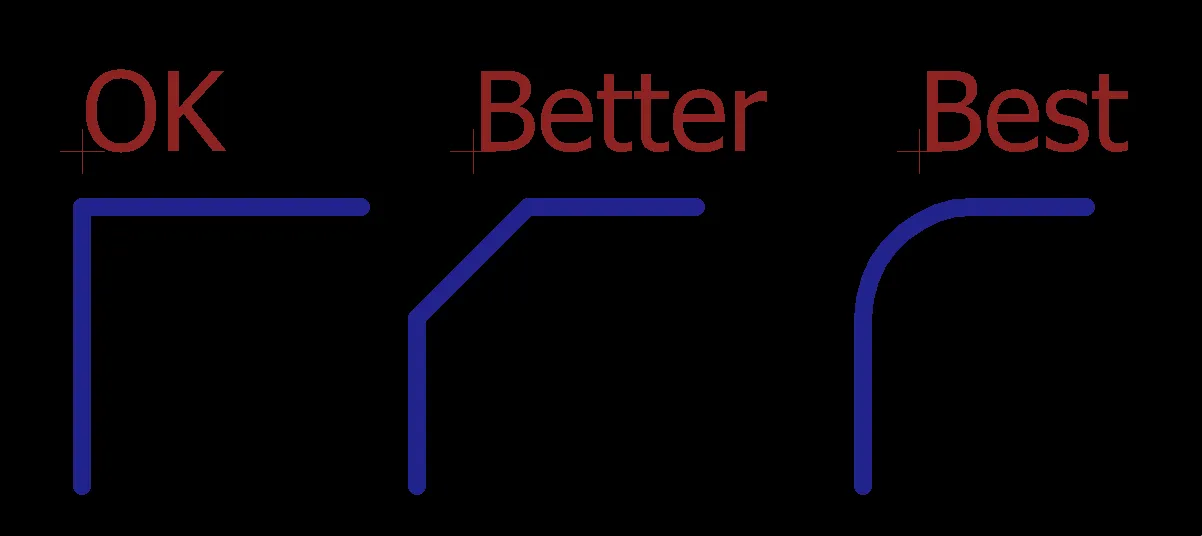
3. Avoid Right-Angle Bends
Sharp 90-degree bends in traces can cause signal reflections and increase EMI radiation due to impedance discontinuities. Instead, use 45-degree angles or smooth curves when changing trace direction. This small adjustment can significantly improve signal integrity.
Controlling PCB Trace Impedance for EMI Reduction
PCB trace impedance is a critical factor in managing signal integrity and reducing EMI. Impedance is the opposition a trace offers to alternating current, and mismatches can cause signal reflections, leading to noise and interference.
On a double-layer PCB, controlling impedance is challenging due to the limited layers for reference planes. However, you can still achieve reasonable results with these techniques:
1. Calculate Trace Width for Target Impedance
Trace impedance depends on its width, thickness, and the dielectric constant of the PCB material (typically FR-4 with a dielectric constant of about 4.2). For a 50-ohm impedance, commonly used in RF and high-speed digital designs, a trace width of around 10-15 mils is typical for a standard 1.6 mm thick board. Use online impedance calculators or simulation tools to fine-tune these values based on your specific stack-up.
2. Maintain Consistent Trace Spacing
For differential pairs or high-speed signals, consistent spacing between traces and their reference plane (usually the ground plane) is essential. Variations in spacing can lead to impedance mismatches, increasing EMI. Aim for a uniform trace-to-ground separation across the board.
3. Use Microstrip Configuration
In double-layer designs, traces on the top layer can be treated as microstrips, with the bottom layer serving as a ground plane. This configuration helps control impedance and reduces EMI by providing a return path for signals directly beneath the trace. For example, a microstrip trace over a ground plane can achieve a controlled 50-ohm impedance with proper width and spacing.
The Role of a PCB Ground Plane in EMI Reduction
A well-designed PCB ground plane is one of the most effective tools for EMI reduction on PCBs. It acts as a low-impedance return path for signals, reducing ground loops and containing electromagnetic fields. Here’s how to optimize your ground plane on a double-layer PCB:
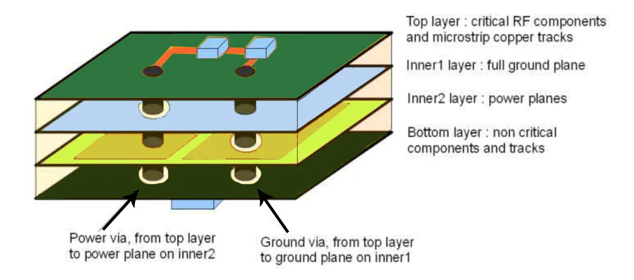
1. Dedicate One Layer to Ground
In a double-layer design, dedicate the bottom layer entirely to a solid ground plane whenever possible. This provides a consistent reference for signals on the top layer and minimizes EMI by offering a direct return path. Avoid breaking the ground plane with traces unless absolutely necessary.
2. Connect Ground Vias Strategically
Use vias to connect ground points on the top layer to the bottom ground plane. Place these vias close to components, especially near high-speed ICs or decoupling capacitors, to minimize return path inductance. For instance, placing a via within 0.1 inches of a capacitor pin can reduce noise significantly.
3. Avoid Ground Plane Splits
Splitting the ground plane to route traces can create discontinuities in the return path, leading to EMI issues. If you must route traces on the ground layer, keep splits minimal and ensure they don’t cross critical signal paths. A solid, unbroken ground plane is ideal for maintaining low noise levels.
Advanced Techniques for EMI Reduction on Double-Layer PCBs
Beyond basic routing and grounding, several advanced strategies can further enhance EMI reduction on PCBs. These techniques are particularly useful for high-speed or mixed-signal designs.
1. Use Decoupling Capacitors Effectively
Decoupling capacitors stabilize power supply lines and reduce noise that contributes to EMI. Place a 0.1 μF capacitor close to each power pin of an IC, ideally within 0.1 inches, to filter high-frequency noise. For lower frequencies, add a larger capacitor, like 10 μF, near the power entry point of the board.
2. Implement Guard Traces
For sensitive signals, consider adding guard traces—grounded traces running parallel to the signal trace. These act as a shield, reducing crosstalk and EMI. Connect guard traces to the ground plane at regular intervals (e.g., every 0.5 inches) using vias to maintain their effectiveness.
3. Route Power Traces Carefully
Power traces can be a significant source of EMI if not routed properly. Keep power traces wide (e.g., 20-30 mils for currents up to 1A) to minimize resistance and inductance. Route them away from sensitive signal traces and place them over the ground plane to reduce noise coupling.
Common Mistakes to Avoid in Double-Layer PCB Trace Routing
Even with the best intentions, certain mistakes can undermine your efforts in double-layer PCB trace routing. Here are pitfalls to watch out for:
- Overcrowding Traces: Trying to fit too many traces in a small area can lead to insufficient spacing, increasing crosstalk and EMI. Plan your layout early to allocate enough space.
- Ignoring Return Paths: Failing to provide a low-impedance return path for signals can cause EMI. Always ensure signals have a nearby ground connection.
- Neglecting Component Placement: Poor placement of components can force long or convoluted trace paths. Place components logically to minimize trace length and crossings.
Tools and Resources for Optimizing Trace Routing
Designing a double-layer PCB with minimal EMI doesn’t have to be a manual process. Several tools can assist in achieving optimal trace routing and impedance control:
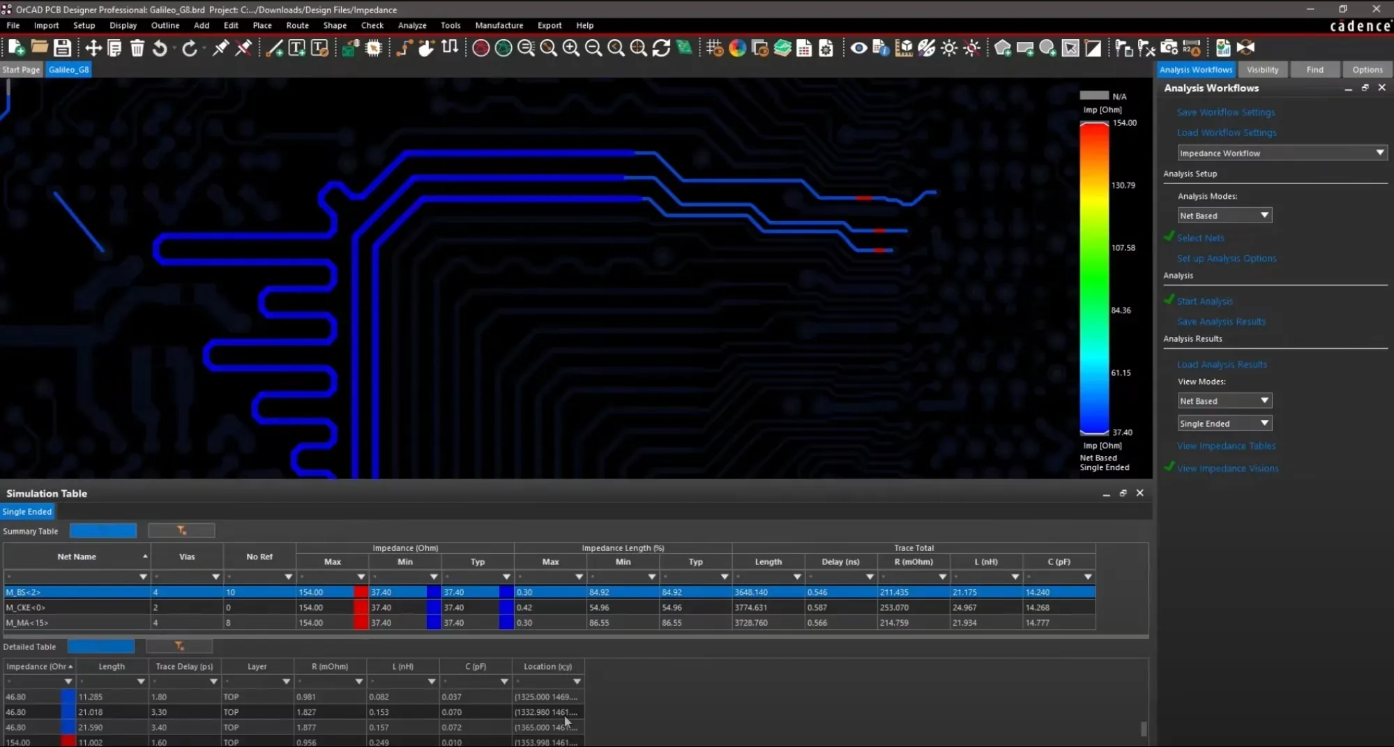
- PCB Design Software: Use advanced software with built-in simulation features to model EMI and impedance before manufacturing.
- Impedance Calculators: Online tools can help determine the correct trace width and spacing for your desired impedance, such as 50 ohms for high-speed signals.
- EMI Simulation Tools: These tools analyze potential EMI issues in your design, allowing you to make adjustments before fabrication.
Conclusion: Mastering Double-Layer PCB Design for EMI Reduction
Mastering the art of double-layer PCB trace routing is essential for creating reliable, high-performance circuits with minimal EMI. By focusing on short and direct traces, controlling PCB trace impedance, leveraging a solid PCB ground plane, and applying advanced EMI reduction on PCB techniques, you can significantly improve your designs. These strategies not only enhance signal integrity but also ensure compliance with electromagnetic compatibility (EMC) standards.


