 ALLPCB


In the world of electronics, designing a printed circuit board (PCB) is both a science and an art. One of the most critical aspects of this process is PCB shape optimization for reducing electromagnetic interference (EMI) and noise. If you're wondering how to achieve cleaner signals and better performance, the answer lies in carefully shaping your PCB and applying smart layout techniques. This blog dives deep into practical strategies for PCB shape EMI reduction, noise reduction PCB layout tips, PCB shape optimization techniques, and grounding strategies for irregular PCBs to help you design boards that perform at their best.
Why PCB Shape Matters for EMI and Noise Reduction
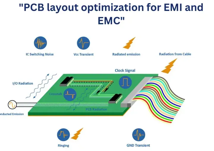
The shape of a PCB isn't just about fitting it into a device; it plays a huge role in controlling EMI and noise. Irregular shapes or poorly planned layouts can create unintended antennas that radiate or pick up electromagnetic interference. Noise, often caused by improper grounding or signal crosstalk, can degrade performance, especially in high-speed or sensitive circuits. By optimizing the PCB shape and layout, you can minimize these issues and ensure reliable operation.
In this guide, we'll explore how shape impacts signal integrity and share actionable techniques to reduce EMI and noise. Whether you're working on a simple prototype or a complex high-density design, these principles will help you achieve better results.
Understanding EMI and Noise in PCB Design
Before diving into optimization techniques, let's break down what EMI and noise mean in the context of PCB design. Electromagnetic interference (EMI) is unwanted electromagnetic energy that disrupts the normal operation of a circuit. It can come from external sources like nearby devices or internal sources like high-speed switching components on the PCB itself. Noise, on the other hand, refers to random or unwanted electrical signals that interfere with the desired signals, often caused by crosstalk, power supply fluctuations, or poor grounding.
For example, in high-speed digital circuits, a signal switching at 100 MHz can generate harmonics that interfere with nearby traces if not managed properly. Similarly, a poorly designed power delivery network might introduce noise, causing voltage drops as high as 0.5V, which can destabilize sensitive components. Addressing these issues starts with the PCB's shape and layout.
Key PCB Shape Optimization Techniques for EMI Reduction
Optimizing the shape of your PCB is a powerful way to reduce EMI. Here are some proven techniques to consider during the design phase:
1. Minimize Loop Areas
Signal loops act like antennas, radiating EMI or picking up interference. When designing your PCB shape, aim to keep signal and return paths as short and direct as possible. For instance, avoid elongated or irregular shapes that force signals to travel long distances. A compact, rectangular PCB often performs better than an irregular, sprawling design because it reduces the loop area.
In practice, if you're working on a high-frequency circuit operating at 500 MHz, reducing the loop area by even 10 square millimeters can significantly lower radiated emissions. Use simulation tools to identify and minimize loop areas during the design phase.
2. Avoid Sharp Corners and Edges
Sharp corners on a PCB can create points of high electric field intensity, leading to EMI radiation. When possible, design your PCB with rounded corners or smooth edges. This is especially important for irregular PCBs where unique shapes are required to fit into specific enclosures. A radius of at least 1 mm on corners can help reduce field concentration and lower EMI risks.
3. Optimize Board Size for Signal Integrity
The overall size of your PCB impacts how signals travel and interact. A board that's too large may introduce longer traces, increasing the risk of noise and EMI. Conversely, a board that's too small can lead to overcrowding, causing crosstalk between traces. Strike a balance by planning the PCB shape to accommodate all components while keeping trace lengths under control. For high-speed designs, aim to keep critical signal traces shorter than one-tenth of the wavelength of the operating frequency to avoid resonance issues.
Noise Reduction PCB Layout Strategies
Beyond shape, the layout of your PCB is crucial for noise reduction. Here are some effective strategies to implement:
1. Separate Analog and Digital Sections
Mixing analog and digital signals on the same plane can lead to noise coupling. When laying out your PCB, create distinct zones for analog and digital components. Use physical separation or split planes to isolate these sections. For example, place analog components like amplifiers on one side of the board and digital components like microcontrollers on the other. This reduces the chance of high-frequency digital noise (e.g., from a 50 MHz clock signal) interfering with sensitive analog signals.
2. Route High-Speed Traces Carefully
High-speed traces are a common source of noise and EMI. Route them away from sensitive areas and avoid crossing over splits in ground planes. Maintain a consistent reference plane beneath high-speed traces to ensure a low-impedance return path. If a trace must cross a plane split, add stitching capacitors (e.g., 0.1 μF) near the crossing to provide a return path for high-frequency currents.
3. Use Proper Trace Spacing
Crosstalk between traces can introduce noise, especially in dense layouts. Follow the 3W rule, which suggests spacing traces at least three times the width of the trace apart. For a trace width of 0.2 mm, maintain a spacing of 0.6 mm to minimize coupling. This is particularly important in irregular PCB shapes where space constraints might tempt you to place traces closer together.
Grounding Strategies for Irregular PCBs
Grounding is one of the most critical factors in reducing EMI and noise, especially for irregular PCBs where standard grounding practices may not apply. Here are some tailored grounding strategies:
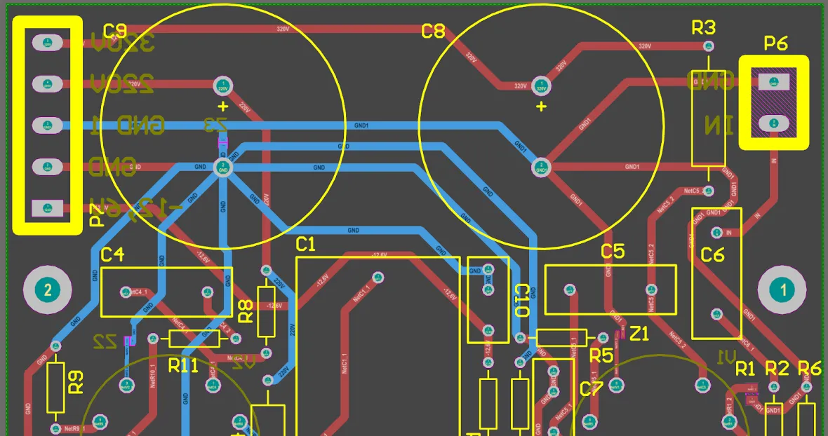
1. Implement a Solid Ground Plane
A continuous ground plane provides a low-impedance path for return currents, reducing noise and EMI. For irregular PCBs, ensure the ground plane follows the board's shape as closely as possible without breaks or splits. If a split is unavoidable due to mixed-signal requirements, use stitching vias or capacitors to connect the planes at high-frequency crossing points. A solid ground plane can reduce noise levels by up to 20 dB in some designs.
2. Use Multiple Ground Vias
In irregular PCBs, components may be placed in unconventional locations, making return paths less predictable. Place multiple ground vias near high-speed components to ensure short, direct connections to the ground plane. For instance, placing 4-6 vias under a high-speed IC can lower the impedance of the return path to below 1 ohm, significantly reducing noise.
3. Isolate Noisy Components
For components that generate significant noise, such as switching regulators, create isolated ground areas connected to the main ground plane at a single point. This "star grounding" technique prevents noise from spreading to sensitive parts of the circuit. On an irregular PCB, plan the shape to accommodate these isolated zones without compromising the overall ground integrity.
Advanced Tips for PCB Shape Optimization
For engineers looking to take their designs to the next level, consider these advanced techniques:
1. Simulate EMI Early in the Design Process
Use electromagnetic simulation software to analyze how your PCB shape affects EMI. These tools can predict radiation patterns and identify problem areas before manufacturing. For example, a simulation might reveal that a specific irregular shape causes a 10 dB increase in radiated emissions at 200 MHz, allowing you to adjust the design accordingly.
2. Incorporate Shielding into the Shape
If EMI remains a concern, design your PCB shape to accommodate shielding cans or enclosures. Leave space around critical components for metal shields that block external interference. This is especially useful for irregular PCBs used in RF applications where external EMI can degrade performance by as much as 30%.
3. Optimize for Manufacturing Constraints
While shape optimization is important, ensure your design is manufacturable. Avoid overly complex shapes that increase production costs or introduce defects. Work with your fabrication partner to balance EMI reduction goals with practical manufacturing limits. For instance, a PCB with a highly irregular shape might require additional routing steps, increasing costs by 15-20%.
Common Mistakes to Avoid in PCB Shape and Layout Design
Even with the best intentions, certain mistakes can undermine your efforts to reduce EMI and noise. Here are some pitfalls to watch out for:
- Ignoring Return Paths: Failing to provide a clear return path for high-frequency signals can lead to increased EMI. Always ensure return currents have a direct route to ground.
- Overcrowding Components: Packing components too tightly, especially on irregular PCBs, can cause crosstalk and heat buildup, amplifying noise issues.
- Neglecting Ground Plane Integrity: Cuts or splits in the ground plane without proper stitching can create high-impedance paths, worsening EMI.
Conclusion: Mastering PCB Shape for Optimal Performance
Optimizing the shape of your PCB is a critical step in reducing EMI and noise, ensuring your designs perform reliably in even the most demanding applications. By focusing on PCB shape EMI reduction, applying noise reduction PCB layout strategies, using PCB shape optimization techniques, and implementing grounding strategies for irregular PCBs, you can create boards that deliver clean signals and minimal interference.
Start by minimizing loop areas, avoiding sharp corners, and balancing board size. Then, refine your layout with proper trace spacing, separated analog and digital zones, and solid grounding practices. For irregular PCBs, tailor your grounding approach to the unique shape while maintaining low-impedance paths. With these techniques, you'll be well on your way to mastering the art of PCB design.
Remember, every design is unique, so test and iterate using simulations and prototypes to fine-tune your approach. By prioritizing signal integrity and EMI control, you'll create PCBs that stand out for their performance and reliability.


