ALLPCB


When designing a printed circuit board (PCB) with edge connectors, one of the most critical factors to consider is the PCB thickness. The standard PCB thickness for edge connectors typically ranges from 1.6mm to 2.4mm, with 1.6mm being the most common choice for compatibility with many connector types. Ensuring the right thickness is essential for proper mating between the PCB and the connector, preventing issues like poor contact, mechanical stress, or signal loss. In this blog, we’ll dive deep into why PCB thickness matters for edge connectors, how to choose the right specifications, and best practices for achieving reliable mating and connector compatibility in PCB design.
Why PCB Thickness Matters for Edge Connectors
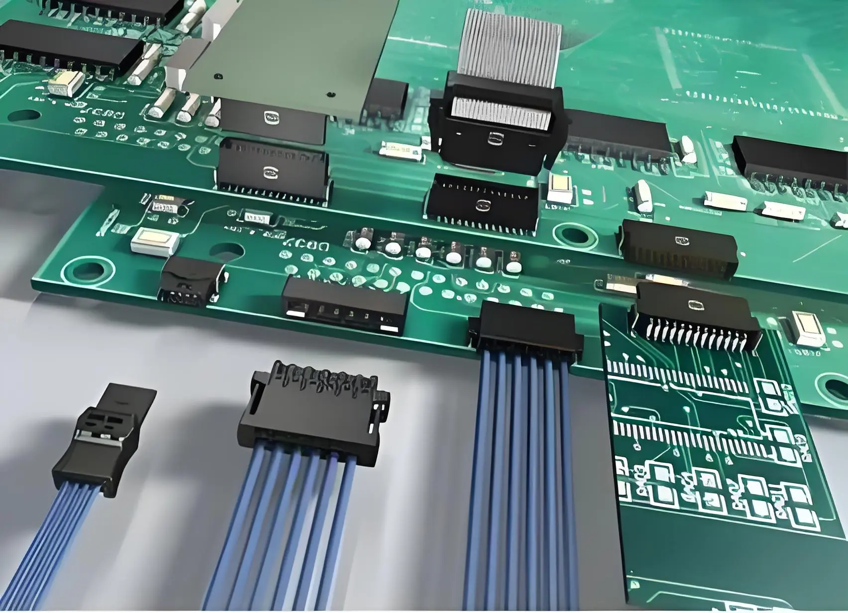
Edge connectors are a popular choice in PCB design due to their simplicity and cost-effectiveness. They allow a PCB to be plugged directly into a mating connector, often used in applications like computer expansion cards, industrial control systems, and consumer electronics. However, for the connection to work seamlessly, the PCB thickness must match the connector’s specifications.
If the PCB is too thin, it may not make proper contact with the connector pins, leading to unreliable connections or signal interruptions. On the other hand, if the PCB is too thick, it can cause excessive force on the connector, potentially damaging both the PCB and the connector over time. Achieving the right balance with standard PCB thickness ensures mechanical stability and electrical reliability.
Standard PCB Thickness for Edge Connectors
The most widely accepted standard PCB thickness for edge connectors is 1.6mm (approximately 0.063 inches). This thickness is compatible with many industry-standard connectors, such as those used in PCI Express cards, ISA slots, and other modular systems. However, depending on the application and connector type, thicknesses of 2.0mm or 2.4mm may also be used, especially in rugged or high-power environments where additional durability is needed.
Here are some common scenarios and their corresponding PCB thickness recommendations:
- Consumer Electronics: 1.6mm is often sufficient for devices like laptops or gaming consoles where space and weight are critical.
- Industrial Applications: 2.0mm to 2.4mm may be preferred for added strength in harsh environments.
- Custom Designs: Always check the connector datasheet for specific thickness tolerances, as some connectors may have a narrow acceptable range (e.g., 1.57mm to 1.63mm for a 1.6mm nominal thickness).
Choosing the right thickness starts with understanding the connector’s design requirements. Most manufacturers provide detailed specifications, including the acceptable PCB thickness range, to ensure proper mating.
Factors Influencing PCB Thickness in Edge Connector Design
Several factors beyond just the connector type can influence the choice of PCB thickness in edge connector designs. Let’s explore these in detail to help you make informed decisions during the design phase.
1. Mechanical Strength and Durability
Thicker PCBs offer more mechanical strength, which is crucial for edge connectors that undergo frequent mating and unmating cycles. For instance, in industrial control systems where boards are swapped often, a 2.0mm or 2.4mm PCB can withstand the physical stress better than a thinner 1.6mm board. However, thicker boards also increase material costs and weight, so balance is key.
2. Signal Integrity and Electrical Performance
PCB thickness can impact signal integrity, especially in high-speed applications. Thicker boards may introduce slight delays in signal transmission due to longer trace paths through vias, while thinner boards can reduce impedance control if not designed properly. For high-speed edge connectors like those in PCIe 4.0 designs, maintaining a standard 1.6mm thickness often aligns with impedance requirements (typically around 85-100 ohms for differential pairs).
3. Connector Compatibility
Not all edge connectors are designed for the same PCB thickness. For example, a connector rated for a 1.6mm board may have a mating tolerance of ±0.1mm. If your PCB falls outside this range, you risk poor contact or damage. Always refer to the connector’s technical documentation to confirm compatibility with your chosen PCB thickness.
Ensuring Proper Mating with Edge Connectors
Proper mating between a PCB and an edge connector goes beyond just selecting the right thickness. It involves careful design and attention to detail to avoid common pitfalls. Below are key strategies to ensure reliable mating in your PCB design.
1. Adhere to Tight Tolerances
Manufacturing tolerances play a significant role in PCB mating. Even a small deviation in thickness (e.g., 0.05mm) can affect how the PCB fits into the connector. Work closely with your fabrication partner to ensure that the final board thickness falls within the connector’s specified range. For a standard 1.6mm PCB, most manufacturers can achieve tolerances of ±0.1mm, which is usually acceptable for most edge connectors.
2. Design Proper Edge Beveling
Edge beveling, or chamfering, refers to the angled cut on the PCB edge that helps guide it into the connector. A typical bevel angle is 30 to 45 degrees, with a depth of about 0.2mm to 0.5mm. This reduces insertion force and prevents damage to both the PCB and connector during mating. Ensure that your design files include clear instructions for beveling to avoid misalignment issues.
3. Optimize Contact Pad Design
The contact pads on the PCB edge must align perfectly with the connector pins for reliable electrical performance. Use a pad width and spacing that matches the connector’s pin layout, typically specified in the datasheet. For example, a standard edge connector might require pads with a width of 1.0mm and a pitch of 2.54mm. Additionally, apply a durable surface finish like gold plating (often 30 microinches over nickel) to enhance wear resistance during repeated mating cycles.
4. Account for Mating Cycles
Edge connectors are rated for a specific number of mating cycles, often ranging from 25 to 500 cycles, depending on the quality and design. High-cycle connectors may require a more robust PCB thickness (e.g., 2.0mm) and a premium surface finish to minimize wear. If your application involves frequent insertions, prioritize durability in both the PCB and connector selection.
Common Challenges in PCB Mating and How to Avoid Them
Even with careful planning, issues can arise during PCB mating with edge connectors. Here are some common challenges and practical solutions to address them.
1. Misalignment During Insertion
Misalignment can cause bent pins or damaged pads. To prevent this, incorporate alignment features like notches or keying slots in your PCB design. These features ensure the board can only be inserted in the correct orientation, reducing the risk of damage.
2. Excessive Insertion Force
If the PCB is too thick or lacks proper beveling, inserting it into the connector may require excessive force, leading to mechanical stress. Always verify the PCB thickness against the connector specs and include a beveled edge to ease insertion.
3. Signal Loss or Intermittent Connections
Poor contact between the PCB pads and connector pins can result in signal loss or intermittent connections. This is often caused by a mismatch in thickness or worn-out pads. Use a high-quality surface finish and regularly inspect the connector and PCB for signs of wear, especially in high-cycle applications.
Best Practices for PCB Design with Edge Connectors
To wrap up, let’s go over some best practices for integrating edge connectors into your PCB design. Following these tips will help ensure long-term reliability and performance.
- Consult Connector Datasheets: Always start with the connector manufacturer’s recommendations for PCB thickness and design parameters.
- Test Prototypes: Before mass production, build and test prototypes to verify proper mating and electrical performance under real-world conditions.
- Consider Environmental Factors: If your PCB will operate in harsh conditions (e.g., high humidity or temperature extremes), opt for a thicker board and protective coatings to enhance durability.
- Collaborate with Fabricators: Work with your PCB fabrication team to confirm that manufacturing tolerances align with your design requirements for edge connectors.

Conclusion: Achieving Reliable Connector Compatibility in PCB Design
Selecting the right PCB thickness for edge connectors is a fundamental step in ensuring proper mating and long-term reliability. The standard thickness of 1.6mm works for most applications, but specific requirements may call for 2.0mm or 2.4mm boards. By paying attention to factors like mechanical strength, signal integrity, and connector compatibility, you can avoid common issues and create a robust design. Additionally, incorporating best practices such as tight tolerances, edge beveling, and optimized contact pads will further enhance the performance of your PCB with edge connectors.
Whether you’re working on consumer electronics or industrial systems, a well-designed PCB with proper mating techniques can make all the difference. Focus on precision in your design process, and you’ll achieve reliable connections that stand the test of time.