ALLPCB


In the world of high-frequency PCB design, every detail matters. One often-overlooked factor that can make or break signal integrity is solder mask thickness. For RF circuits, where precision is key, the thickness of the solder mask, along with its dielectric constant, directly impacts signal loss, impedance control, and overall performance. So, how does solder mask thickness affect high-frequency PCBs, and why should you care? Simply put, a well-chosen solder mask thickness ensures minimal signal loss and maintains impedance, which are critical for reliable RF performance.
In this detailed guide, we’ll dive deep into the role of solder mask thickness in high-frequency PCB design. We’ll explore its effects on signal integrity, discuss optimal thickness ranges for RF circuits, and provide actionable insights on managing signal loss and impedance control. Whether you’re an engineer working on cutting-edge RF designs or a hobbyist looking to optimize your next project, this post will equip you with the knowledge to make informed decisions.
What Is Solder Mask and Why Does It Matter in High-Frequency PCBs?
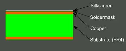
Solder mask is a thin protective layer applied over the copper traces of a printed circuit board (PCB). Its primary job is to prevent short circuits by insulating the traces and protecting them from environmental factors like moisture and dust. It also helps during soldering by ensuring solder only sticks to designated pads. While these functions are vital for any PCB, solder mask takes on an even more critical role in high-frequency designs, such as those used in RF circuits.
In high-frequency PCB design, signals travel at incredibly fast speeds, often in the range of gigahertz (GHz). At these frequencies, even small variations in materials or dimensions can disrupt signal integrity. The solder mask, though thin, sits directly on or near the copper traces, influencing the electromagnetic fields around them. Its thickness and dielectric properties can alter how signals propagate, leading to potential issues like signal loss or impedance mismatch if not carefully managed.
The Role of Solder Mask Thickness in Signal Integrity
Signal integrity refers to the quality and reliability of an electrical signal as it travels through a circuit. In high-frequency PCBs, maintaining signal integrity is a challenge due to factors like crosstalk, noise, and signal loss. Solder mask thickness plays a surprisingly significant role in this equation.
When designing for RF circuits, engineers often aim for a controlled impedance—typically 50 ohms for most RF applications. The solder mask, being a dielectric material, affects the capacitance between the trace and the surrounding environment. A thicker solder mask increases capacitance, which can lower the impedance of the trace. Conversely, a thinner solder mask reduces capacitance, potentially raising impedance. If not accounted for, this can lead to mismatches, causing reflections and degrading signal quality.
For example, a standard solder mask thickness of 0.8 to 1.2 mils (20-30 micrometers) might work fine for low-frequency designs. However, in RF circuits operating at 5 GHz or higher, even a 0.2-mil variation can shift impedance by 1-2 ohms, enough to cause noticeable signal degradation. This is why precise control over solder mask thickness for RF circuits is essential.
Solder Mask Dielectric Constant and Its Impact on Signal Loss
Beyond thickness, the solder mask dielectric constant (often denoted as Dk) is another critical factor in high-frequency PCB design. The dielectric constant measures a material’s ability to store electrical energy in an electric field. For solder masks, Dk typically ranges from 3.5 to 4.5, depending on the material and manufacturer specifications.
A higher dielectric constant means the solder mask can store more energy, which slows down the signal and increases the risk of signal loss due to solder mask. This loss, often referred to as dielectric loss, becomes more pronounced at higher frequencies. For instance, at 10 GHz, a solder mask with a Dk of 4.0 might contribute to a signal loss of 0.02 dB per inch, while a lower Dk of 3.5 could reduce this loss by 20-30% under the same conditions.
Choosing a solder mask with a lower dielectric constant can help minimize signal loss, but it often comes at a higher cost. Additionally, the thickness of the mask interacts with its Dk. A thicker mask with a high Dk amplifies dielectric loss, while a thinner mask can mitigate some of these effects. Balancing these factors is a key part of optimizing RF performance.
Optimal Solder Mask Thickness for RF Circuits
So, what is the ideal solder mask thickness for RF circuits? The answer depends on the specific requirements of your design, including operating frequency, trace geometry, and impedance targets. However, general guidelines can help steer you in the right direction.
For most high-frequency applications, a solder mask thickness of 0.5 to 0.8 mils (12-20 micrometers) is often recommended. This range strikes a balance between providing adequate protection and minimizing impact on signal integrity. Thinner masks reduce capacitance and dielectric loss, which is beneficial for RF signals operating above 1 GHz. However, going too thin—below 0.5 mils—can compromise the mask’s protective capabilities, risking damage to traces during handling or assembly.
In some cases, designers opt to remove solder mask entirely from critical RF traces, exposing the bare copper. While this eliminates dielectric loss and impedance variations caused by the mask, it leaves traces vulnerable to oxidation and environmental damage. If bare traces are used, a surface finish like ENIG (Electroless Nickel Immersion Gold) is often applied for protection, though this introduces its own set of variables to consider in impedance calculations.
Signal Loss Due to Solder Mask: How to Minimize It
As mentioned earlier, signal loss due to solder mask is a significant concern in high-frequency PCB design. This loss occurs primarily through two mechanisms: dielectric loss (due to the mask’s material properties) and conductor loss (influenced by the mask’s interaction with the trace). Here are some practical steps to minimize these effects:
- Choose Low-Loss Materials: Opt for solder mask materials with a lower dielectric constant and dissipation factor (Df). A Df below 0.02 is ideal for RF applications, as it indicates lower energy loss.
- Control Thickness: Work with your PCB manufacturer to ensure consistent solder mask thickness within the optimal range of 0.5-0.8 mils for RF designs.
- Partial Masking: Consider applying solder mask only to non-critical areas, leaving RF traces exposed or covered with a minimal layer if protection is needed.
- Simulate and Test: Use simulation tools to model the impact of solder mask on signal loss before fabrication. Tools like electromagnetic field solvers can predict how different thicknesses and materials affect performance at your target frequency.
By taking these steps, you can significantly reduce signal degradation and ensure your high-frequency PCB performs as intended.
Impedance Control with Solder Mask in High-Frequency Designs
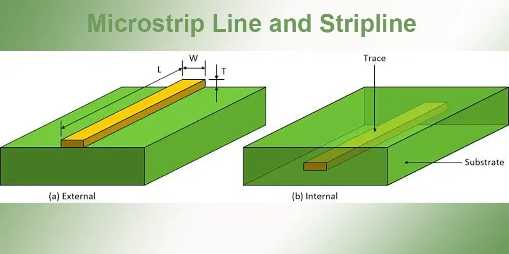
Impedance control with solder mask is a cornerstone of successful high-frequency PCB design. As signals travel along a trace, they encounter a characteristic impedance determined by the trace width, substrate height, dielectric constant of the substrate, and—yes—the solder mask. Mismatched impedance leads to signal reflections, which can distort waveforms and degrade performance.
For a typical 50-ohm microstrip line on a standard FR-4 substrate (Dk of 4.4), a solder mask thickness of 1 mil might lower the impedance by 1-3 ohms due to increased capacitance. While this may seem minor, even small deviations can cause issues in RF systems where tight tolerances are required. To achieve precise impedance control with solder mask, consider the following:
- Adjust Trace Geometry: If a thicker solder mask is unavoidable, you can compensate by slightly widening the trace or adjusting the substrate height to maintain the desired impedance.
- Use Simulation Software: Tools like field solvers can help calculate the exact impact of solder mask thickness on impedance, allowing for fine-tuned designs.
- Specify Tolerances: Communicate with your PCB fabricator to ensure tight control over solder mask application, specifying a target thickness and acceptable variation (e.g., ±0.1 mil).
Challenges in High-Frequency PCB Design with Solder Mask
Designing for high-frequency PCB design comes with unique challenges, and solder mask is often at the center of these issues. One common problem is inconsistency in mask application. Variations in thickness across the board can lead to uneven impedance and signal loss, especially in large or complex designs. Working with a reliable manufacturer who can guarantee uniform application is crucial.
Another challenge is the trade-off between protection and performance. While a thicker solder mask offers better insulation and durability, it increases dielectric loss and alters impedance. On the other hand, a thinner mask or no mask at all improves electrical performance but leaves traces vulnerable. Finding the right balance often requires iterative testing and close collaboration with your fabrication team.
Finally, environmental factors like temperature and humidity can affect solder mask performance over time. At high frequencies, even small changes in the mask’s dielectric properties due to moisture absorption can impact signal integrity. Selecting high-quality, stable materials designed for RF applications can mitigate these risks.
Practical Tips for Engineers Working on RF PCBs
If you’re diving into high-frequency PCB design, here are some actionable tips to optimize solder mask usage for better signal integrity:
- Collaborate Early: Engage with your PCB manufacturer during the design phase to understand their solder mask capabilities and material options.
- Prioritize Low-Dk Materials: Invest in solder mask materials with a dielectric constant below 4.0 for frequencies above 5 GHz to minimize signal loss.
- Document Specifications: Clearly define solder mask thickness and tolerances in your design files to avoid surprises during production.
- Test Prototypes: Build and test prototypes to validate your design assumptions, especially if you’re pushing frequency limits or using unconventional stackups.
These steps can save time and resources while ensuring your RF circuits perform reliably under real-world conditions.
Conclusion: Mastering Solder Mask for High-Frequency Success
In the intricate world of high-frequency PCB design, solder mask thickness is far more than a minor detail—it’s a critical factor in achieving optimal signal integrity. From influencing impedance to contributing to signal loss, the solder mask plays a pivotal role in the performance of RF circuits. By understanding and controlling solder mask thickness for RF circuits, considering the solder mask dielectric constant, and addressing signal loss due to solder mask, engineers can unlock the full potential of their designs.
Whether you’re fine-tuning impedance control with solder mask or navigating the challenges of high-frequency PCB design, the insights and tips shared in this guide can help you make informed decisions. Remember, precision is everything in RF design, and even the smallest layer—like the solder mask—can make a big difference. Partner with a trusted PCB fabrication service to ensure your specifications are met, and don’t hesitate to simulate and test your designs to achieve the best results.
By mastering the unsung hero of solder mask thickness, you’re one step closer to creating high-performing, reliable RF circuits that stand the test of time.