ALLPCB


When it comes to manual PCB assembly, the silkscreen layer is a vital tool for ensuring accuracy and efficiency. A well-designed silkscreen provides clear instructions and component identification, reducing errors during assembly. So, how do you optimize silkscreen readability for manual PCB assembly? The key lies in adhering to specific design rules for PCB silkscreen character size, silkscreen spacing requirements, silkscreen color contrast, and following readability guidelines for PCB design. In this comprehensive guide, we’ll dive into actionable manual assembly silkscreen tips to help you create effective silkscreen layouts that streamline the assembly process.
Why Silkscreen Readability Matters in Manual PCB Assembly
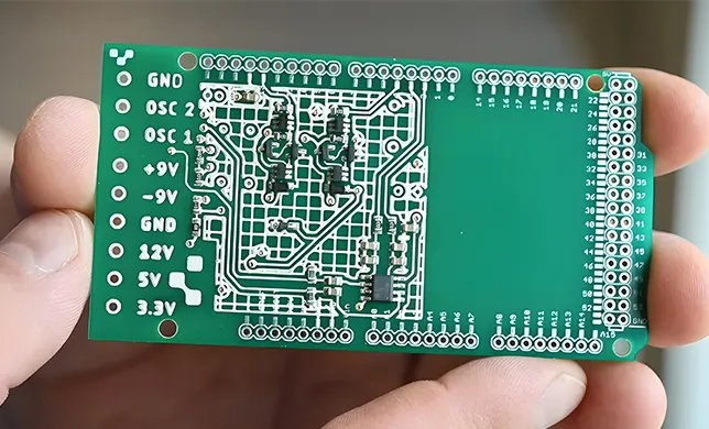
In manual PCB assembly, technicians rely heavily on the silkscreen layer to identify components, understand polarity, and follow placement instructions. A poorly designed silkscreen with tiny text, unclear spacing, or low contrast can lead to mistakes, delays, and increased costs. On the other hand, a clear and optimized silkscreen acts as a visual guide, ensuring components like resistors, capacitors, and ICs are placed correctly the first time. By focusing on readability, you can minimize errors and improve the overall efficiency of the assembly process.
Let’s explore the essential design rules to achieve optimal silkscreen readability for manual assembly, covering character size, spacing, color contrast, and more.
1. PCB Silkscreen Character Size: Ensuring Legible Text
One of the most critical factors in silkscreen readability is the size of the characters. If the text is too small, assemblers may struggle to read it, especially under typical workshop lighting conditions or when working with densely populated boards. Here are some specific guidelines for PCB silkscreen character size:
- Minimum Height: Characters should be at least 1.5 mm (0.06 inches) tall to ensure legibility. Some industry standards suggest a minimum of 1.0 mm, but for manual assembly, larger text is always better.
- Stroke Width: The thickness of the lines forming each character should be at least 0.15 mm (0.006 inches). Thin lines can blur or fade during the printing process, making text harder to read.
- Font Choice: Use simple, sans-serif fonts like Arial or Helvetica. These fonts avoid intricate details that might not print clearly on a PCB surface.
For example, when labeling a resistor as “R1,” ensure the text height is at least 1.5 mm to allow assemblers to read it without straining their eyes. If space is limited, prioritize critical labels over less essential ones, but never compromise on the minimum size.
By adhering to these character size rules, you create a silkscreen that supports quick and accurate component identification during manual assembly.
2. Silkscreen Spacing Requirements: Avoiding Clutter
Proper spacing between characters, words, and other silkscreen elements is just as important as character size. Overcrowded text or symbols can confuse assemblers, leading to misinterpretation. Here are the key silkscreen spacing requirements to follow:
- Character Spacing: Maintain a minimum spacing of 0.2 mm (0.008 inches) between individual characters to prevent them from blending together during printing.
- Element Spacing: Keep at least 0.5 mm (0.02 inches) between text and nearby components, pads, or other silkscreen markings. This prevents overlap and ensures clarity.
- Component Boundaries: Avoid placing text directly over component footprints or solder pads. Instead, position labels adjacent to the relevant component, ideally pointing to the correct pin or polarity marker.
For instance, when labeling a capacitor with “C1” and indicating its polarity with a “+” symbol, ensure there’s enough space between the text and symbol to avoid confusion. Proper spacing helps assemblers quickly distinguish between different elements on the board.

3. Silkscreen Color Contrast: Maximizing Visibility
The color of the silkscreen ink plays a significant role in how easily it can be read against the PCB background. Poor contrast can make text and symbols nearly invisible, especially under varying lighting conditions. Here are some tips for optimizing silkscreen color contrast:
- Standard Colors: White silkscreen ink is the most common choice for green or blue solder masks, as it provides a high contrast ratio. Yellow ink can also be used for darker backgrounds, though it’s less common.
- Contrast Ratio: Aim for a contrast ratio of at least 3:1 between the silkscreen ink and the PCB background. This aligns with accessibility guidelines for visibility and ensures text stands out.
- Avoid Low-Contrast Combinations: Don’t use light-colored ink on light backgrounds or dark ink on dark backgrounds. For example, black silkscreen on a dark green solder mask can be nearly impossible to read.
In manual assembly environments, where lighting may not always be ideal, high contrast is non-negotiable. For example, on a standard green PCB, white silkscreen text for labels like “R2” or “GND” will be far more visible than gray or beige ink. Always test your color choices under different lighting conditions to confirm readability.
4. Readability Guidelines for PCB Silkscreen Design
Beyond character size, spacing, and color, there are additional readability guidelines for PCB silkscreen design that can enhance clarity during manual assembly. These guidelines focus on the overall layout and content of the silkscreen layer:
- Prioritize Essential Information: Only include critical details like component designators (e.g., “R1,” “C2”), polarity markers, and pin numbers. Avoid cluttering the board with unnecessary text, such as long descriptions or redundant labels.
- Use Consistent Orientation: Orient text in a uniform direction, ideally readable from a single perspective (e.g., left to right, top to bottom). Avoid rotating text at odd angles unless absolutely necessary for space constraints.
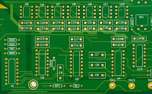
- Group Related Information: Place labels close to the components they describe. For example, position the label “D1” next to its diode and include a small arrow or line to indicate the anode or cathode if polarity matters.
- Include Polarity and Orientation Markers: For components like diodes, LEDs, and electrolytic capacitors, always add clear symbols (e.g., “+” for positive, “-” for negative) to prevent assembly errors.
Following these guidelines ensures that assemblers can quickly interpret the silkscreen without second-guessing the meaning of labels or symbols. A well-organized silkscreen layer acts as a roadmap, guiding technicians through the assembly process with minimal confusion.
5. Manual Assembly Silkscreen Tips: Best Practices for Success
In addition to the core design rules, here are some practical manual assembly silkscreen tips to further optimize your PCB for hands-on assembly:
- Limit Text Density: Avoid overcrowding the board with too much text. If a board is densely populated, consider using a separate assembly drawing or documentation for non-critical information rather than cramming it onto the silkscreen.
- Test Print Quality: Before finalizing your design, request a sample or prototype to check the silkscreen print quality. Ensure that characters are sharp, not blurry, and that spacing and contrast meet your expectations.
- Account for Manufacturing Tolerances: Silkscreen printing isn’t always perfectly aligned. Leave a buffer zone of at least 0.3 mm (0.012 inches) around text to account for slight misalignments during production.
- Use Reference Designators: Stick to standard reference designators like “R” for resistors, “C” for capacitors, and “U” for ICs. These are universally understood and reduce the learning curve for assemblers.
- Highlight Critical Test Points: Mark test points with clear labels like “TP1” or “GND” to assist with debugging and testing after assembly. Use a distinct symbol, such as a small circle, to make them stand out.
By incorporating these tips, you can create a silkscreen layer that not only supports assembly but also aids in troubleshooting and quality control. For example, clearly marked test points can save hours during post-assembly testing by guiding technicians directly to the correct locations.
Common Silkscreen Design Mistakes to Avoid
Even with the best intentions, certain silkscreen design mistakes can undermine readability and lead to assembly errors. Here are some pitfalls to watch out for:
- Text Over Components: Placing text directly over component footprints or solder pads can make it unreadable after assembly. Always position labels outside the component area.
- Overloading with Information: Including too much detail, like full component values or lengthy notes, can clutter the board and distract from essential information.
- Ignoring Contrast Issues: Choosing a silkscreen color that blends into the solder mask can render labels invisible. Always prioritize high contrast over aesthetic preferences.
- Inconsistent Labeling: Using different naming conventions or orientations for similar components can confuse assemblers. Maintain consistency across the board.
Avoiding these mistakes ensures that your silkscreen remains a helpful tool rather than a source of frustration during manual assembly.
Conclusion: Designing Silkscreen for Seamless Manual Assembly
Creating a silkscreen layer that optimizes readability for manual PCB assembly is all about attention to detail. By focusing on PCB silkscreen character size, adhering to silkscreen spacing requirements, ensuring high silkscreen color contrast, and following readability guidelines for PCB design, you can significantly reduce assembly errors and improve efficiency. The manual assembly silkscreen tips provided in this guide offer actionable steps to refine your design process and create boards that are easy to work with.
Remember, the silkscreen is more than just a decorative layer—it’s a critical communication tool between the designer and the assembler. Investing time in optimizing its readability pays off in faster assembly times, fewer mistakes, and a smoother production process. Whether you’re designing a simple prototype or a complex multilayer board, these silkscreen design rules will help ensure success every step of the way.