 ALLPCB


When it comes to designing printed circuit boards (PCBs), especially for high-frequency applications, two critical factors often come into play: prepreg thickness and dielectric constant (Dk value). These elements directly influence signal integrity, impedance control, and overall PCB performance. At ALLPCB, we understand the importance of optimizing these parameters to ensure your designs meet the highest standards. In this blog, we’ll explore how prepreg Dk value and prepreg thickness impact PCB performance, and provide actionable insights for achieving the best results in your projects, particularly in high-frequency PCB design.
What Are Prepreg and Dielectric Constant in PCB Design?
Before diving into the details, let’s clarify the basics. Prepreg, short for "pre-impregnated," is a fiberglass material soaked in resin and used as an insulating layer between copper layers in a PCB. It bonds the layers together during the lamination process and plays a vital role in determining the board’s thickness and electrical properties. The dielectric constant (Dk) of prepreg refers to its ability to store electrical energy in an electric field, which affects how signals travel through the board. A lower Dk value typically means faster signal transmission, which is crucial for high-frequency applications.
Understanding and controlling both prepreg thickness and Dk is essential for optimizing PCB material properties and ensuring reliable performance. Let’s break down these concepts further and see how they impact your designs.
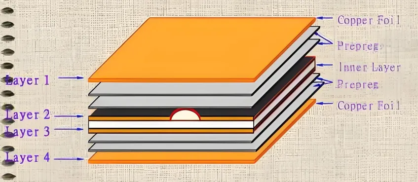
Why Prepreg Thickness Matters in PCB Design
Prepreg thickness is a key factor in determining the overall thickness of a PCB and the spacing between conductive layers. This spacing influences several performance aspects, including impedance, signal integrity, and PCB thermal management. Here’s why it’s so important:
- Impedance Control: In high-frequency designs, maintaining consistent impedance is critical for signal integrity. Prepreg thickness directly affects the distance between signal traces and ground planes, which in turn impacts characteristic impedance. For example, a thinner prepreg layer reduces the distance, lowering impedance, while a thicker layer increases it. Designers often target specific impedance values, such as 50 ohms for many RF applications, by carefully selecting prepreg thickness.
- Signal Integrity: Thicker prepreg can lead to higher signal delays due to increased dielectric material between layers. Conversely, thinner prepreg reduces delays but may increase crosstalk if layers are too close. Balancing thickness is key for high-frequency PCB design.
- Thermal and Mechanical Stability: Thicker prepreg layers can improve thermal dissipation and mechanical strength, which are vital for boards exposed to high temperatures or physical stress. However, excessive thickness can make the board bulky and less suitable for compact designs.
For instance, in a 4-layer PCB stackup designed for a 5 GHz application, a prepreg thickness of 0.2 mm between layers might be chosen to achieve a specific impedance while keeping signal loss minimal. Adjusting this value even slightly can alter performance, so precision is essential.
The Role of Dielectric Constant (Dk) in Prepreg Materials
The dielectric constant prepreg value, often abbreviated as Dk, is a measure of how much a material can store electrical energy compared to a vacuum. In PCB design, the Dk value of prepreg materials significantly affects signal speed and loss, especially in high-frequency applications. Here’s a closer look at its impact:
- Signal Speed: A lower Dk value allows signals to travel faster through the material because it reduces the capacitance between traces. For high-frequency designs, materials with a Dk value between 2.2 and 3.0 are often preferred over standard materials with Dk values of 4.4 to 4.8, as they minimize signal delay. For example, at 10 GHz, a material with a Dk of 2.5 can reduce signal propagation delay by up to 30% compared to a material with a Dk of 4.5.
- Signal Loss: Materials with lower Dk values typically have a lower dissipation factor (Df), which means less signal loss due to energy absorption. This is critical for maintaining signal integrity over long traces in high-frequency circuits.
- Impedance Matching: The Dk value influences the characteristic impedance of transmission lines. A mismatch in Dk between prepreg and other materials in the stackup can cause reflections and signal degradation.
Choosing the right prepreg Dk value is a balancing act. While low-Dk materials improve performance, they can be more expensive and harder to process. Standard materials with higher Dk values are more cost-effective but may not meet the demands of high-speed or high-frequency applications.
How Prepreg Thickness and Dk Interact in High-Frequency PCB Design
In high-frequency PCB design, the relationship between prepreg thickness and Dk becomes even more critical. These two factors work together to determine how signals behave as they travel through the board. Here’s how their interaction impacts performance:
- Combined Effect on Impedance: Both thickness and Dk value affect the impedance of a transmission line. For a given trace width, a thinner prepreg with a higher Dk increases capacitance, lowering impedance. Conversely, a thicker prepreg with a lower Dk decreases capacitance, raising impedance. Designers use simulation tools to model these effects and select the optimal combination for their specific frequency range.
- Signal Delay and Loss: At frequencies above 1 GHz, even small variations in prepreg thickness or Dk can cause noticeable signal delays or losses. For example, in a 10 GHz design, a 0.1 mm difference in prepreg thickness paired with a Dk shift from 3.0 to 3.5 can increase signal delay by several picoseconds, potentially disrupting timing in critical applications.
- Crosstalk and Noise: Thinner prepreg layers with high Dk values can increase crosstalk between adjacent traces due to higher capacitance. In contrast, thicker layers with low Dk values reduce crosstalk but may not be feasible in compact designs where space is limited.
To optimize performance, designers must carefully select materials and stackups that balance these factors based on the operating frequency and application requirements. For instance, in a 5G communication board, a combination of thin prepreg (0.15 mm) and a low-Dk material (Dk of 2.8) might be used to minimize loss and maintain tight impedance control.
Choosing the Right Prepreg Materials for Optimal PCB Performance
Selecting the appropriate prepreg material involves evaluating both thickness and Dk based on your design needs. Here are some practical tips for making the right choice:
- Match Material to Frequency: For low-frequency applications (below 1 GHz), standard prepreg materials with Dk values around 4.4 and moderate thickness (0.2-0.3 mm) are often sufficient. For high-frequency designs (above 1 GHz), consider advanced materials with Dk values below 3.0 and thinner layers (0.1-0.2 mm) to reduce signal loss.
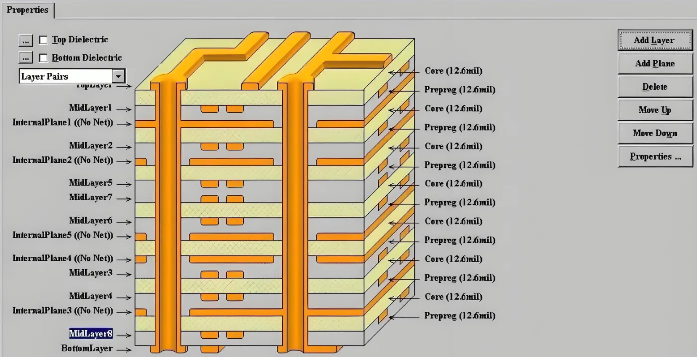
- Consider Stackup Design: In multilayer boards, ensure that prepreg thickness and Dk are consistent across layers to avoid impedance mismatches. Use simulation software to test different stackup configurations before manufacturing.
- Balance Cost and Performance: Low-Dk materials and ultra-thin prepreg layers can significantly improve performance but often come at a higher cost. Evaluate whether the performance gains justify the added expense for your specific application.
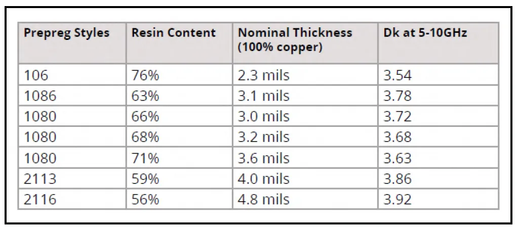
- Consult Material Data Sheets: Always review the manufacturer’s data for PCB material properties, including Dk, dissipation factor, and available thicknesses. These specs will help you predict how the material will behave in your design.
At ALLPCB, we offer a wide range of prepreg materials and thicknesses to support your design goals, whether you’re working on a simple prototype or a complex high-frequency board. Our team can assist in selecting the best options to meet your performance and budget requirements.
Suggested Reading: Prepreg vs. Core: Understanding PCB Layer Stackup Materials
Best Practices for High-Frequency PCB Design
Designing PCBs for high-frequency applications requires attention to detail beyond just prepreg selection. Here are some additional best practices to ensure optimal performance:
- Minimize Fiber Weave Effect: The fiberglass weave in prepreg can cause variations in Dk along a trace, leading to signal skew in differential pairs. Rotate trace routing or use materials with uniform weave patterns to mitigate this issue.
- Use Controlled Impedance Routing: Design traces with precise widths and spacing to match the target impedance, factoring in prepreg thickness and Dk. For example, a 50-ohm trace at 5 GHz might require a width of 0.3 mm with a 0.2 mm prepreg layer of Dk 3.0.
- Optimize Ground Planes: Solid ground planes reduce noise and improve signal return paths. Ensure that prepreg thickness between signal layers and ground planes is consistent to maintain uniform impedance.
- Test and Validate: Use simulation tools to model signal behavior before fabrication. After manufacturing, perform tests like time-domain reflectometry (TDR) to verify impedance and signal integrity.
By following these practices and carefully managing prepreg thickness and Dk, you can achieve reliable performance even in the most demanding high-frequency applications.
Common Challenges and How to Overcome Them
Even with careful planning, designers often face challenges related to prepreg and dielectric properties. Here are some common issues and solutions:
- Inconsistent Dk Across Layers: Variations in Dk between prepreg batches can disrupt impedance. Work with a reliable supplier to ensure material consistency, and specify tight tolerances for Dk in your design requirements.
- Difficulty in Achieving Thin Layers: Ultra-thin prepreg layers can be hard to handle and may increase manufacturing defects. If thin layers are necessary, collaborate closely with your fabrication partner to ensure process capability.
- Signal Loss at High Frequencies: If losses are higher than expected, consider switching to a prepreg with a lower Dk and Df. Even a small reduction, such as from Dk 3.5 to 3.0, can make a noticeable difference at frequencies above 5 GHz.
Addressing these challenges early in the design phase can save time and reduce costly revisions during production.
Conclusion: Optimize Your PCB with the Right Prepreg Choices
In the world of PCB design, small details like prepreg thickness and dielectric constant can make a big difference in performance, especially for high-frequency applications. By understanding how these factors interact and influence signal integrity, impedance, and overall board reliability, you can make informed decisions to optimize your designs. Whether you’re aiming for minimal signal loss in a 5G application or tight impedance control in an RF circuit, selecting the right prepreg Dk value and thickness is a critical step.
At ALLPCB, we’re committed to supporting your success with high-quality materials and expert guidance. By leveraging the insights shared in this blog, you can enhance your high-frequency PCB design process and achieve outstanding results. Remember to balance performance needs with practical considerations like cost and manufacturability, and always validate your choices through simulation and testing.
With the right approach to PCB material properties, your designs can reach their full potential, delivering the speed, reliability, and efficiency required in today’s advanced electronics.


