 ALLPCB


Are you struggling with PCB silkscreen registration issues that lead to assembly errors? Achieving precise silkscreen alignment is critical for error-free PCB assembly. In this comprehensive guide, we’ll dive into the importance of silkscreen alignment, explore techniques for high-accuracy printing, and share best practices to ensure perfect registration every time. Whether you’re a design engineer or a manufacturing professional, this blog will equip you with the knowledge to minimize errors and enhance assembly efficiency.
What Is PCB Silkscreen and Why Does Alignment Matter?
PCB silkscreen, often called the legend layer, is the printed text, symbols, and markings on a printed circuit board’s surface. This layer serves as a visual guide, identifying components, test points, polarity markers, and assembly instructions. While it doesn’t play a functional role in the board’s electrical performance, its accuracy is vital for seamless manufacturing and assembly processes.
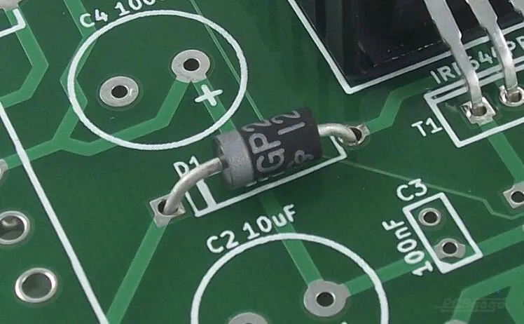
Misaligned silkscreen can cause significant problems, such as confusion during component placement, incorrect polarity orientation, or even delays in troubleshooting. For instance, if a silkscreen label for a capacitor is offset by just 0.5 mm, an assembler might misplace the component, leading to potential circuit failure. Proper silkscreen alignment tolerance ensures that every marking is exactly where it needs to be, reducing the risk of costly PCB assembly errors.
The Challenges of PCB Silkscreen Registration
PCB silkscreen registration refers to the precise alignment of the silkscreen layer with the underlying board features, such as copper traces, pads, and vias. Achieving perfect registration is challenging due to several factors:
- Manufacturing Tolerances: Even small deviations in printing equipment or board fabrication can result in misaligned silkscreen layers. Typical alignment tolerances for silkscreen are around ±0.1 mm to ±0.2 mm, but high-density designs may require tighter precision.
- Material Shrinkage: During the PCB fabrication process, materials like FR-4 can shrink or expand due to heat and pressure, affecting layer alignment.
- Complex Designs: Boards with fine-pitch components or high component density leave little room for error, making silkscreen alignment even more critical.
- Human and Machine Errors: Manual processes or outdated printing equipment can introduce inconsistencies in silkscreen placement.
These challenges highlight the need for robust techniques and tools to ensure high-accuracy silkscreen printing and minimize errors during assembly.
Key Techniques for High-Accuracy Silkscreen Printing
To achieve precise PCB silkscreen alignment, manufacturers and designers must adopt advanced techniques and best practices. Below are some proven methods to ensure perfect registration:
1. Use of Fiducial Markers for Alignment
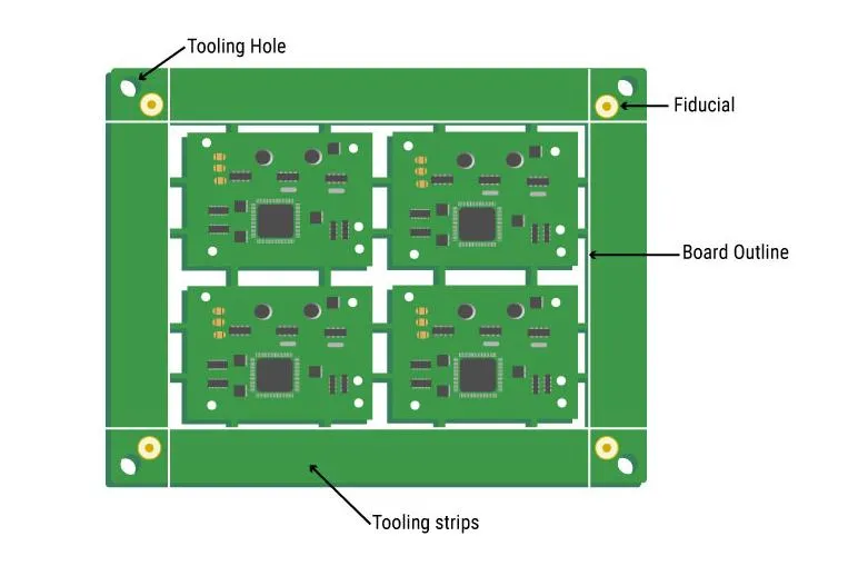
Fiducial markers are small reference points etched into the copper layer of a PCB. These markers act as alignment guides for both the silkscreen printing process and automated assembly equipment. By placing fiducials in at least three non-collinear positions on the board, manufacturers can achieve alignment accuracy within ±0.05 mm. This method significantly reduces the risk of silkscreen layer misalignment.
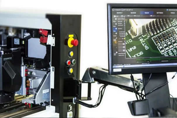
2. Automated Optical Inspection (AOI)
Automated Optical Inspection systems use high-resolution cameras to verify silkscreen alignment against the design file. AOI can detect offsets as small as 0.01 mm, ensuring that the silkscreen layer matches the board’s layout with exceptional precision. Incorporating AOI into the manufacturing workflow helps catch alignment issues before they lead to assembly errors.
3. Advanced Printing Technologies
Modern silkscreen printing methods, such as inkjet printing, offer superior accuracy compared to traditional screen printing. Inkjet systems can achieve resolutions up to 720 DPI, allowing for crisp, precise markings even on high-density boards. This technology minimizes the risk of smudging or misalignment, which is common with older techniques.
4. Tight Silkscreen Alignment Tolerance Standards
Establishing strict silkscreen alignment tolerance standards is essential for consistent quality. For most applications, a tolerance of ±0.1 mm is acceptable, but for high-reliability industries like aerospace or medical devices, tolerances as tight as ±0.05 mm may be necessary. Designers should specify these tolerances in their fabrication notes to ensure manufacturers meet the required precision.
Silkscreen Layer Alignment Best Practices
Beyond advanced techniques, following best practices during design and manufacturing can further improve silkscreen alignment and prevent PCB assembly errors. Here are actionable tips for engineers and manufacturers:
1. Optimize Silkscreen Design in CAD Software
Start by ensuring that your silkscreen layer is correctly aligned with other layers in your PCB design software. Use grid snapping and alignment tools to place markings precisely over pads and components. Additionally, maintain a minimum clearance of 0.2 mm between silkscreen text and copper features to avoid overlap during printing.
2. Specify Silkscreen Requirements in Fabrication Files
Clearly communicate your silkscreen alignment requirements in the fabrication files. Include details such as acceptable tolerances, preferred printing methods, and any specific alignment markers. Providing a detailed readme file alongside your Gerber files can help manufacturers understand your expectations and reduce the likelihood of errors.
3. Minimize Silkscreen Complexity
Overloading the silkscreen layer with unnecessary text or graphics can increase the risk of misalignment. Focus on essential information, such as component designators, polarity indicators, and test points. Use standard font sizes (e.g., 0.8 mm height) and line widths (e.g., 0.15 mm) to ensure legibility and alignment accuracy.
4. Collaborate with Your Manufacturer
Work closely with your PCB manufacturer to understand their capabilities and limitations regarding silkscreen printing. Request a design for manufacturability (DFM) review to identify potential alignment issues before production begins. This collaboration can save time and prevent costly rework due to silkscreen errors.
5. Test and Validate with Prototypes
Before moving to full-scale production, order a small batch of prototypes to validate silkscreen alignment. Inspect the boards under magnification to check for offsets or inconsistencies. If issues are detected, adjust the design or printing process to achieve the desired accuracy.
Common PCB Assembly Errors Caused by Silkscreen Misalignment
Poor silkscreen registration can lead to a range of assembly errors, impacting both time-to-market and product reliability. Here are some common issues and how they relate to silkscreen alignment:
- Component Misplacement: If silkscreen markings are offset, assemblers may place components in the wrong orientation or location. For example, a misaligned polarity marker on a diode could result in reverse installation, causing circuit failure.
- Delayed Debugging: Incorrect or unclear silkscreen labels can make it difficult to identify test points or components during troubleshooting, leading to longer debug times.
- Increased Rework Costs: Assembly errors due to silkscreen misalignment often require rework, increasing labor costs and delaying production schedules. Studies suggest that rework can account for up to 10% of total manufacturing costs in some cases.
The Role of Silkscreen in High-Reliability Applications
In industries like automotive, aerospace, and medical devices, the stakes for PCB assembly accuracy are even higher. A single assembly error due to silkscreen misalignment could lead to catastrophic failures. For example, in a medical device PCB, a misplaced component caused by unclear silkscreen markings could compromise patient safety.
For high-reliability applications, silkscreen alignment best practices must be paired with rigorous quality control measures. Manufacturers often use advanced AOI systems and X-ray inspection to verify alignment and component placement. Additionally, silkscreen materials should be chosen for durability, ensuring that markings remain legible even under harsh environmental conditions.
How to Measure and Improve Silkscreen Alignment Accuracy
Measuring silkscreen alignment accuracy is a critical step in quality assurance. Here’s how to do it effectively:
- Use Precision Measurement Tools: Employ digital microscopes or coordinate measuring machines (CMM) to measure the offset between silkscreen markings and reference features like fiducials. Aim for measurements accurate to within 0.01 mm.
- Compare Against Design Files: Overlay the fabricated board’s silkscreen layer with the original design file to identify discrepancies. Many AOI systems can automate this comparison process.
- Track and Analyze Defects: Maintain a log of silkscreen alignment issues across production batches. Use statistical process control (SPC) to identify trends and implement corrective actions.
- Continuous Improvement: Regularly update printing equipment and train staff on the latest silkscreen alignment techniques to maintain high accuracy over time.
By consistently measuring and refining the silkscreen process, manufacturers can achieve near-perfect registration and reduce the incidence of PCB assembly errors.
Conclusion: Mastering PCB Silkscreen Alignment for Flawless Assembly
Precision PCB silkscreen alignment is a cornerstone of error-free assembly. By understanding the challenges of silkscreen registration, adopting high-accuracy printing techniques, and following silkscreen layer alignment best practices, designers and manufacturers can significantly reduce assembly errors and improve product reliability. From using fiducial markers and AOI systems to optimizing designs and collaborating with manufacturers, every step counts in achieving perfect registration.
At ALLPCB, we’re committed to helping you achieve the highest standards in PCB manufacturing. By focusing on silkscreen alignment tolerance and leveraging cutting-edge technology, we ensure that your boards are assembled with precision and efficiency. Whether you’re working on a simple prototype or a complex high-reliability design, mastering silkscreen alignment is key to success.


