 ALLPCB


In the world of PCB design, power plane vias play a critical role in ensuring signal integrity and reliable performance. If you're wondering how to optimize power plane via placement for signal integrity, the answer lies in strategic positioning, understanding current capacity, and minimizing inductance. Proper via stitching and adherence to placement guidelines can significantly reduce noise, improve power delivery, and enhance overall circuit stability. In this comprehensive guide, we'll dive deep into the best practices for power plane via stitching, explore via current capacity, discuss via inductance, and provide actionable via placement guidelines to help you achieve optimal signal integrity in your designs.
What Are Power Plane Vias and Why Do They Matter?
Power plane vias are small conductive pathways in a printed circuit board (PCB) that connect power and ground planes across different layers. These vias are essential for delivering power to components and maintaining a stable reference for signals. Without proper placement, power plane vias can introduce noise, increase inductance, and degrade signal integrity, leading to performance issues in high-speed or high-current applications.
Signal integrity refers to the quality of an electrical signal as it travels through a circuit. Poor signal integrity can result in data errors, timing issues, and electromagnetic interference (EMI). By optimizing power plane via placement, you create a low-impedance path for power delivery and reduce unwanted noise, ensuring that signals remain clean and reliable.
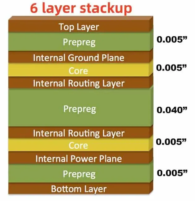
Understanding Power Plane Via Stitching
Power plane via stitching involves placing multiple vias strategically around a PCB to connect power or ground planes across layers. This technique is commonly used to create a robust power distribution network (PDN) and minimize impedance. Via stitching helps in reducing voltage drops, improving current distribution, and lowering EMI by providing multiple low-resistance paths for current to flow.
In high-speed designs, via stitching is particularly important near high-current components like microprocessors or FPGAs. For example, placing vias at regular intervals (e.g., every 0.5 inches) around a power plane can reduce loop inductance and ensure stable voltage delivery. Without proper stitching, you risk creating "hot spots" where current density is too high, leading to overheating or signal degradation.
Key Tip: When implementing power plane via stitching, use a grid pattern for uniform current distribution. Ensure that vias are placed close to component power pins to minimize the distance current must travel.
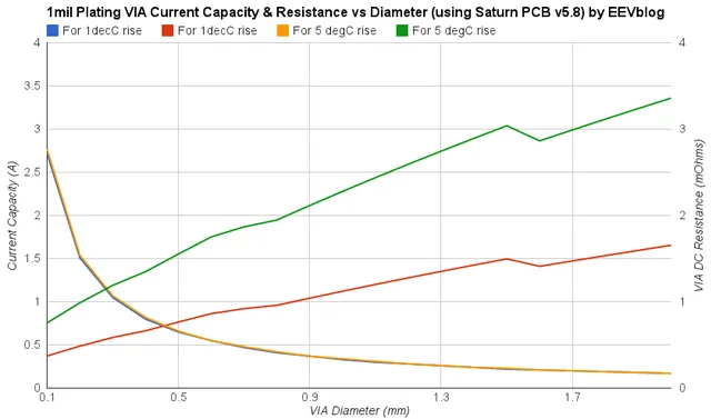
Power Plane Via Current Capacity: How Much Can They Handle?
One of the most critical factors in power plane via design is understanding their current capacity. The amount of current a via can handle depends on its diameter, plating thickness, and the material used. A typical via with a diameter of 10 mils (0.010 inches) and standard copper plating can safely carry around 1-2 amperes of current. However, for high-current applications, you may need larger vias or multiple vias in parallel to distribute the load.
To calculate the current capacity, you can use industry-standard formulas or refer to PCB design guidelines. For instance, the current-carrying capacity increases with the via's cross-sectional area. Doubling the diameter of a via can increase its current capacity by a factor of four. However, thermal considerations are equally important. Excessive current through a via can cause overheating, leading to reliability issues. As a rule of thumb, keep the current density below 500 A/in2 to avoid thermal stress.
Practical Example: If you're designing a board for a power supply delivering 10 amperes, using five 12-mil vias in parallel (each handling 2 amperes) can effectively distribute the load and prevent overheating.
Power Plane Via Inductance: Minimizing the Impact
Inductance in power plane vias is a major concern for signal integrity, especially in high-speed designs. Via inductance can cause voltage fluctuations and delay power delivery to components, leading to signal distortion. The inductance of a via depends on its length, diameter, and proximity to other conductive elements. A shorter, wider via generally has lower inductance.
For instance, a typical via with a length of 50 mils and a diameter of 10 mils might have an inductance of around 1-2 nH (nanohenries). While this may seem small, in high-frequency circuits operating at 1 GHz or above, even a small inductance can create significant impedance, disrupting power delivery.
Best Practice: To minimize power plane via inductance, use the shortest possible via length by connecting power planes on adjacent layers. Additionally, place multiple vias in parallel to reduce the effective inductance. For critical high-speed signals, aim for via inductance below 0.5 nH by optimizing the via size and layer stackup.
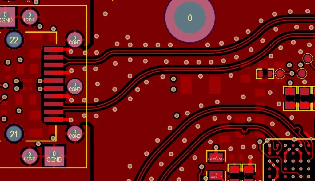
Via Placement Guidelines for Optimal Signal Integrity
Proper via placement is the cornerstone of maintaining signal integrity in PCB designs. Misplaced vias can introduce noise, increase impedance, and create ground bounce. Below are some key via placement guidelines to follow for power plane vias:
- Place Vias Close to Power Pins: Position power plane vias as close as possible to the power pins of ICs and other high-current components. This reduces the loop area and minimizes inductance. For example, placing a via within 50 mils of a power pin can significantly improve power delivery.
- Use Multiple Vias for High-Current Paths: For components requiring more than 1 ampere, use multiple vias in parallel to distribute current evenly and reduce thermal stress.
- Avoid Vias in Signal Paths: Keep power plane vias away from high-speed signal traces to prevent interference. If unavoidable, ensure a solid ground plane is nearby to shield the signal.
- Stitch Ground Planes Regularly: In multilayer boards, stitch ground planes with vias at regular intervals (e.g., every 0.2-0.5 inches) to maintain a low-impedance return path for signals.
- Consider Via Aspect Ratio: Ensure the via’s height-to-diameter ratio (aspect ratio) is below 10:1 to maintain manufacturability and reliability. High aspect ratios can lead to plating defects.
By following these via placement guidelines, you can create a robust power distribution network that supports signal integrity and prevents performance issues.
Signal Integrity Vias: Special Considerations
Signal integrity vias are specifically used to maintain the quality of high-speed signals by providing a clean return path and reducing crosstalk. Unlike power plane vias, which focus on current delivery, signal integrity vias are often placed near differential pairs or high-speed traces to control impedance and minimize reflections.
For instance, in a design with a 10 Gbps signal, placing ground vias adjacent to signal vias can help maintain a controlled impedance of 50 ohms, reducing signal distortion. Additionally, signal integrity vias should be placed symmetrically around differential pairs to balance the return paths and prevent skew.
Key Tip: Use simulation tools to analyze the impact of via placement on signal integrity. Tools can help you model impedance mismatches and optimize via locations before fabrication.
Common Mistakes to Avoid in Power Plane Via Design
Even experienced designers can make mistakes when placing power plane vias. Here are some common pitfalls to watch out for:
- Insufficient Via Stitching: Failing to use enough vias for power or ground planes can lead to high impedance and voltage drops. Always use a grid pattern for stitching in high-current areas.
- Overloading a Single Via: Relying on a single via for high current can cause overheating and failure. Distribute the load across multiple vias.
- Ignoring Layer Transitions: Poorly planned via transitions between layers can introduce inductance and disrupt signal integrity. Keep transitions short and direct.
- Neglecting Thermal Management: High-current vias generate heat. Ensure proper spacing and consider thermal vias if heat dissipation is a concern.
By avoiding these mistakes, you can ensure a more reliable and efficient PCB design.
Tools and Techniques for Optimizing Via Placement
Modern PCB design software offers powerful tools to help optimize power plane via placement. Features like auto-placement, impedance calculators, and thermal analysis can streamline the design process. Additionally, running simulations for signal integrity and power distribution can identify potential issues before manufacturing.
For example, simulating a power plane with vias spaced at different intervals can reveal the optimal configuration for minimizing voltage drops. A common target is to keep voltage ripple below 1% of the supply voltage (e.g., 50 mV for a 5V rail) by adjusting via placement and count.
Practical Tip: Use design rule checks (DRC) to ensure vias meet manufacturing constraints, such as minimum spacing and aspect ratio, to avoid fabrication issues.
Conclusion: Achieving Signal Integrity with Power Plane Vias
Optimizing power plane via placement is a fundamental step in achieving signal integrity in PCB designs. By focusing on power plane via stitching, understanding via current capacity, minimizing via inductance, and following via placement guidelines, you can create a robust power distribution network that supports clean signals and reliable performance. Whether you're working on high-speed digital circuits or high-current power supplies, the principles of signal integrity vias remain the same: strategic placement, careful planning, and attention to detail.
With the actionable tips and best practices shared in this guide, you're well-equipped to tackle the challenges of power plane via design. Implementing these strategies will not only enhance the performance of your PCBs but also reduce the risk of costly redesigns. Keep experimenting with different layouts and simulations to find the perfect balance for your specific application.


