 ALLPCB


In the world of printed circuit board (PCB) manufacturing, fine-pitch surface mount technology (SMT) assembly is becoming increasingly common due to the demand for smaller, more powerful devices. Components like Quad Flat No-Lead (QFN) and Ball Grid Array (BGA) packages require precision to ensure reliable connections and performance. One critical element in achieving this precision is the use of Liquid Photoimageable (LPI) solder mask. But how does LPI solder mask contribute to optimizing fine-pitch SMT assembly? Simply put, LPI solder mask offers superior accuracy in defining solderable areas, prevents solder bridging, and supports the tight tolerances needed for components with pitches as small as 0.4mm or less. In this blog, we’ll dive deep into the role of LPI solder mask in fine-pitch assembly, focusing on its application for QFN and BGA components, aperture size considerations, and the importance of solder mask defined pads.
What is Liquid Photoimageable Solder Mask and Why Does It Matter?
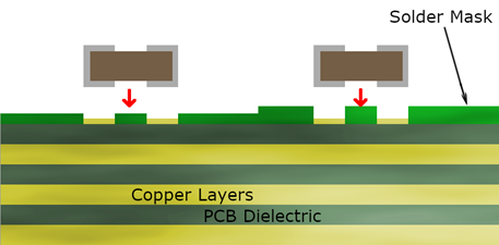
Liquid Photoimageable (LPI) solder mask is a type of protective coating applied to PCBs during manufacturing. Unlike traditional dry film solder masks, LPI is applied as a liquid and then exposed to light through a photographic process to create precise patterns. This results in a thin, uniform layer that protects copper traces from oxidation and prevents solder from flowing where it shouldn’t during assembly.
For fine-pitch SMT assembly, where component leads or pads are spaced extremely close together (often below 0.5mm), precision is everything. LPI solder mask excels in this area because it can achieve resolutions down to 50 micrometers, allowing for accurate alignment with tiny pads and tight spaces. This makes it an ideal choice for modern, high-density PCB designs that incorporate QFN and BGA components.
The Challenges of Fine-Pitch SMT Assembly
Fine-pitch SMT assembly involves placing components with very small lead spacing or pad sizes onto a PCB. For example, QFN packages often have lead pitches of 0.4mm or 0.5mm, while BGA components can have ball pitches as tight as 0.3mm. At these scales, even minor errors in solder application or mask alignment can lead to issues like solder bridging, insufficient solder joints, or misalignment during reflow.
Without a properly designed solder mask, the risk of defects increases significantly. Solder can flow between closely spaced pads, creating shorts, or fail to adhere properly, leading to weak connections. This is where LPI solder mask comes into play, offering the precision and control needed to mitigate these risks.
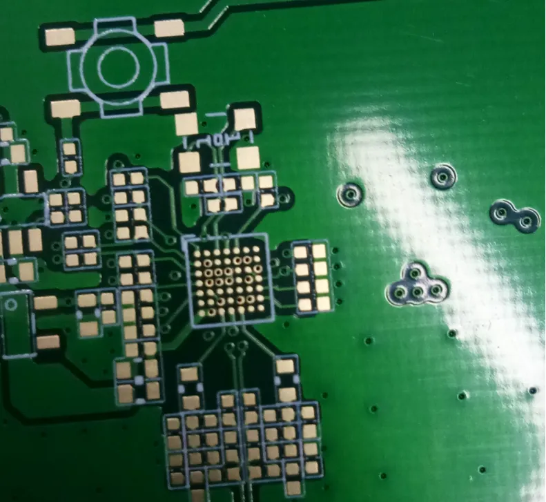
LPI Solder Mask for QFN Components: Precision in Tight Spaces
QFN packages are popular in modern electronics due to their small size and excellent thermal performance. However, their lack of protruding leads and tight pad spacing make assembly challenging. The solder mask must define the exact areas where solder should be applied, ensuring that each pad is isolated from its neighbors to prevent bridging.
Using LPI solder mask for QFN components allows manufacturers to create highly precise openings, often referred to as solder mask apertures. These openings are tailored to match the pad size and spacing of the QFN, typically with tolerances as tight as ±25 micrometers. This level of accuracy ensures that solder paste is deposited only where needed, reducing the risk of defects during reflow. For a 0.4mm pitch QFN, the solder mask aperture might be designed to be 0.05mm smaller than the pad on each side to prevent overflow while still allowing a strong joint.
LPI Solder Mask for BGA Components: Supporting High-Density Connections
BGA components present their own set of challenges in fine-pitch SMT assembly. With hundreds or even thousands of tiny solder balls arranged in a grid under the package, the solder mask must create precise openings for each ball while maintaining isolation between them. A pitch of 0.5mm or less leaves little room for error, as even a slight misalignment can cause solder to bridge between balls, leading to electrical shorts.
LPI solder mask for BGA components is designed to handle these high-density layouts. Its photoimageable nature allows for the creation of small, consistent apertures—sometimes as small as 0.2mm in diameter—for each solder ball. This ensures that solder paste is applied uniformly and only in the intended areas. Additionally, LPI solder mask can be applied in thinner layers (typically 10-20 micrometers) compared to traditional masks, reducing the risk of solder mask residue interfering with the BGA balls during placement.
Solder Mask Aperture Size: Getting the Balance Right
The size of the solder mask aperture is a critical factor in fine-pitch SMT assembly. If the aperture is too large, excess solder can flow out, risking bridges between pads. If it’s too small, there may not be enough solder to form a reliable joint, leading to weak connections or voids.
For fine-pitch components, the solder mask aperture size is often designed to be slightly smaller than the pad itself. A common guideline is to reduce the aperture by 0.025mm to 0.05mm per side compared to the pad dimensions. For instance, on a 0.3mm wide pad for a QFN component, the solder mask aperture might be set to 0.25mm to control solder flow. This reduction, often called “solder mask expansion,” helps confine the solder paste during reflow while still providing enough material for a strong bond.
LPI solder mask excels in achieving these tight tolerances due to its high-resolution imaging process. Unlike traditional masks, which may struggle with apertures smaller than 0.1mm, LPI can consistently produce openings as small as 0.075mm, making it ideal for fine-pitch designs.
Solder Mask Defined Pads: Enhancing Control in Fine-Pitch Assembly
In fine-pitch SMT assembly, solder mask defined (SMD) pads are often used to improve control over solder application. With SMD pads, the solder mask overlaps the edges of the copper pad, creating a smaller exposed area for soldering. This overlap acts as a barrier, preventing solder from spreading beyond the intended area and reducing the risk of bridging in tight spaces.
LPI solder mask is particularly effective for creating SMD pads because of its precision. For a 0.4mm pitch component, the solder mask might overlap the pad by 0.05mm on each side, leaving a solderable area of just 0.3mm. This tight control is essential for preventing defects in high-density layouts. Additionally, SMD pads help ensure consistent solder joint heights, which is critical for components like BGAs where uneven joints can lead to reliability issues.
However, the design of solder mask defined pads must be carefully balanced. Overlapping too much can restrict solder flow, leading to insufficient joints, while too little overlap may not provide enough control. Using advanced design software, manufacturers can simulate and optimize these dimensions to achieve the best results with LPI solder mask.
Benefits of LPI Solder Mask in Fine-Pitch SMT Assembly
The advantages of using LPI solder mask in fine-pitch SMT assembly are numerous, making it a preferred choice for high-density PCB designs. Here are some key benefits:
- High Precision: LPI solder mask can achieve resolutions down to 50 micrometers, allowing for accurate definition of small pads and tight pitches (e.g., 0.3mm or less).
- Reduced Solder Bridging: By precisely controlling aperture sizes and pad definitions, LPI minimizes the risk of solder flowing between closely spaced pads.
- Thin and Uniform Application: With typical thicknesses of 10-20 micrometers, LPI solder mask avoids interference with component placement, especially for low-profile packages like QFN.
- Compatibility with High-Density Designs: LPI supports the intricate layouts required for modern electronics, accommodating hundreds of connections in a small area, as seen with BGA components.
- Improved Reliability: Consistent solder joints and reduced defect rates lead to more reliable PCBs, critical for applications in automotive, medical, and consumer electronics.
Best Practices for Using LPI Solder Mask in Fine-Pitch Assembly
To maximize the benefits of LPI solder mask in fine-pitch SMT assembly, manufacturers and designers should follow these best practices:
- Optimize Aperture Design: Work with your PCB manufacturer to fine-tune solder mask aperture sizes based on component pitch and pad dimensions. For a 0.5mm pitch BGA, consider an aperture diameter of 0.25mm to 0.3mm to balance solder volume and control.
- Use Solder Mask Defined Pads: For pitches below 0.5mm, implement SMD pads with a mask overlap of 0.025mm to 0.05mm per side to prevent bridging.
- Ensure Accurate Registration: During the LPI application process, precise alignment between the mask and the PCB is crucial to avoid misalignment of apertures, especially for fine-pitch components.
- Test and Validate: Before full production, create prototypes to test solder mask performance with specific components. Use X-ray inspection for BGAs to verify joint quality under the package.
- Collaborate with Experts: Partner with experienced PCB manufacturing teams to leverage their expertise in LPI solder mask application for fine-pitch designs.
Conclusion: Elevating Fine-Pitch SMT Assembly with LPI Solder Mask
As electronics continue to shrink in size while growing in complexity, fine-pitch SMT assembly has become a cornerstone of modern PCB manufacturing. Components like QFN and BGA packages demand precision at every stage, from design to soldering. Liquid Photoimageable solder mask plays a pivotal role in meeting these demands by providing unparalleled accuracy in defining solderable areas, controlling aperture sizes, and supporting solder mask defined pads.
Whether it’s preventing solder bridging on a 0.4mm pitch QFN or ensuring uniform joints on a high-density BGA, LPI solder mask delivers the reliability and performance needed for today’s advanced designs. By understanding its capabilities and following best practices, designers and manufacturers can optimize their fine-pitch SMT assembly processes, resulting in higher quality and more dependable electronic products.


