 ALLPCB


If you're new to printed circuit boards (PCBs) and wondering what "mils" means when it comes to copper thickness, you're in the right place. Simply put, "mils" is a unit of measurement equal to one-thousandth of an inch (0.001 inch), often used to describe the thickness of copper layers on a PCB. Understanding copper thickness, measured in mils or ounces per square foot (oz/ft2), is crucial for designing boards that can handle the right amount of current and perform reliably. In this beginner-friendly guide, we'll break down PCB copper thickness explained, dive into mils in PCB design, explore copper weight for hobbyists, cover PCB copper basics, and help with understanding PCB layers. Let's get started on this journey to mastering the essentials of PCB design.
Why Copper Thickness Matters in PCB Design
Copper is the backbone of any PCB, acting as the conductive material that carries electrical signals and power between components. The thickness of this copper layer directly affects how much current the board can handle, how well it dissipates heat, and how durable it is. For hobbyists and beginners, choosing the right copper thickness can mean the difference between a functioning prototype and a burnt-out board.
Typically, copper thickness is discussed in two ways: as a weight (ounces per square foot) or as a direct measurement (mils or micrometers). A standard PCB often uses 1 oz/ft2 of copper, which translates to about 1.37 mils or 35 micrometers of thickness. But why does this matter? Thicker copper can carry more current without overheating, while thinner copper might be better for fine traces in compact designs. Understanding these basics helps you make informed decisions for your projects.
Breaking Down the Terms: Mils, Ounces, and Micrometers
Let's clear up the confusion around the units used to measure copper thickness in PCBs. As a beginner, you might hear terms like "mils," "ounces," or "micrometers" thrown around. Here's what they mean:
- Mils: A mil is one-thousandth of an inch (0.001 inch). It's a common unit in the PCB industry, especially in the United States, to describe the thickness of copper layers. For example, 1.37 mils is the thickness of 1 oz/ft2 copper.
- Ounces per Square Foot (oz/ft2): This is a weight measurement that indicates how much copper is spread over one square foot of the board. It's an indirect way to talk about thickness. A 1 oz/ft2 copper layer weighs 1 ounce when spread over a square foot and equals about 1.37 mils in thickness.
- Micrometers (μm): This metric unit is often used outside the U.S. and equals one-millionth of a meter. Since 1 mil is about 25.4 micrometers, a 1 oz/ft2 layer (1.37 mils) is roughly 35 μm thick.
Most PCB manufacturers will assume 1 oz/ft2 (1.37 mils or 35 μm) as the default copper thickness unless you specify otherwise. As a hobbyist, starting with this standard is often a safe bet for simple projects like LED circuits or microcontroller boards.
PCB Copper Basics: How Thickness Affects Performance
Now that you know the units, let's dive into how copper thickness impacts your PCB's performance. There are three main factors to consider:
1. Current Carrying Capacity
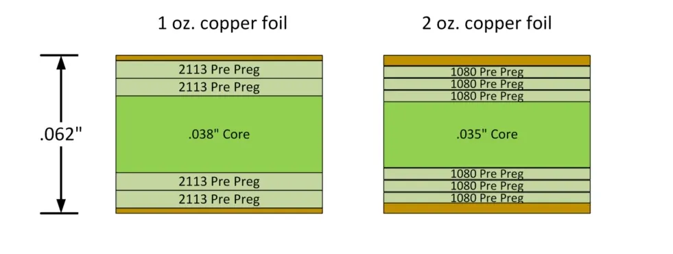
The thicker the copper, the more current it can carry without overheating. For example, a trace on a 1 oz/ft2 copper layer can safely handle about 1-2 amps of current, depending on the trace width (say, 10 mils wide at 1 amp). If your project involves high-power components like motors or power supplies, you might need 2 oz/ft2 (2.74 mils or 70 μm) or even 3 oz/ft2 (4.11 mils or 105 μm) to handle currents up to 5-10 amps or more.
2. Heat Dissipation
Thicker copper also helps spread heat better. If your circuit generates a lot of heat—think of high-speed processors or power converters—a thicker copper layer can prevent hot spots that might damage components. For instance, a 2 oz/ft2 layer dissipates heat more effectively than a 0.5 oz/ft2 layer (0.685 mils or 17.5 μm), which is often used in low-power, lightweight designs.
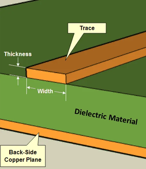
3. Trace Width and Spacing
Thinner copper layers are often used for finer traces and tighter spacing, which is crucial for compact or high-density designs. However, thin copper can't carry as much current, so there's a trade-off. For hobbyists working on small boards, sticking to 1 oz/ft2 usually offers a good balance between trace size and current capacity.
Related Reading: The Ultimate Guide to PCB Trace Width for Beginners
Copper Weight for Hobbyists: Choosing the Right Thickness
As a hobbyist, you might wonder which copper thickness is best for your project. Here's a simple guide to help you decide based on common use cases:
- 0.5 oz/ft2 (0.685 mils or 17.5 μm): This is a lightweight option, often used for low-current, high-density designs. It's great for small signal circuits like sensors or audio projects, but not suitable for power-heavy applications.
- 1 oz/ft2 (1.37 mils or 35 μm): The industry standard and the most common choice for hobbyists. It works well for general-purpose projects like Arduino-based circuits, LED lighting, or simple power supplies handling up to 2-3 amps with proper trace widths.
- 2 oz/ft2 (2.74 mils or 70 μm): Choose this for higher current needs, such as power electronics or motor drivers. It can handle around 5-6 amps on wider traces but increases the cost of fabrication.
- 3 oz/ft2 or more (4.11 mils or 105 μm+): Used in specialized, high-power applications like industrial equipment. This is rarely needed for hobbyist projects due to cost and manufacturing complexity.
Remember, thicker copper means higher costs, so balance your needs with your budget. For most beginner projects, 1 oz/ft2 is a safe and affordable starting point.
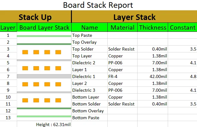
Understanding PCB Layers and Copper Thickness
PCBs aren't just about a single layer of copper. Many boards have multiple layers, each with its own copper thickness, depending on the design. Let's explore how copper thickness ties into understanding PCB layers.
Single-Layer vs. Multi-Layer PCBs
A single-layer PCB has copper on just one side of the board, often used for very simple circuits. Here, the copper thickness (like 1 oz/ft2) applies to that one layer. Multi-layer PCBs, common in complex electronics, have copper on both sides or even sandwiched between insulating layers. Each layer might have the same or different copper thicknesses. For example, outer layers might use 1 oz/ft2 for signal traces, while inner layers for power planes might use 2 oz/ft2 to handle higher currents.
Inner vs. Outer Layers
In multi-layer boards, outer layers are typically thinner after manufacturing due to processes like etching and plating. If you start with 1 oz/ft2 copper, the finished outer layer might be closer to 1.2-1.4 oz/ft2 after plating. Inner layers, however, often maintain their specified thickness. As a hobbyist, you might not need to worry about this for simple 2-layer boards, but it’s good to know if you’re stepping into more advanced designs.
How to Specify Copper Thickness for Your PCB
When ordering a PCB, you’ll need to tell the manufacturer what copper thickness you want. Most online platforms allow you to select from standard options like 0.5 oz, 1 oz, or 2 oz per square foot. If you're unsure, stick with 1 oz/ft2 for general projects. Here's how to approach this as a beginner:
- Check Your Design Needs: Estimate the current your traces will carry. Online calculators can help determine if 1 oz/ft2 is enough or if you need thicker copper based on trace width and current.
- Consider Cost: Thicker copper increases manufacturing costs. For hobbyist budgets, start with standard options unless your project demands more.
- Communicate Clearly: When submitting your design files, include a note or use the order form to specify copper weight (e.g., "1 oz/ft2 for all layers").
If you're designing for high-frequency signals, like in RF circuits, copper thickness also affects impedance. For instance, a 50-ohm impedance trace on a 1 oz/ft2 layer might need a specific width (often around 60 mils on FR-4 material) to maintain signal integrity. Tools like impedance calculators can help with this, but that’s a more advanced topic for later.
Related Reading: PCB Copper Thickness in PCB Design
Common Mistakes to Avoid with Copper Thickness
As a beginner, it's easy to make mistakes when dealing with copper thickness. Here are a few pitfalls to watch out for:
- Underestimating Current Needs: If your traces carry more current than the copper can handle, they can overheat and fail. Always double-check with a current capacity chart or calculator.
- Ignoring Heat Issues: Thin copper might not dissipate heat well in power-heavy designs, leading to component damage. When in doubt, go slightly thicker.
- Over-specifying Thickness: Choosing 2 oz/ft2 or more when 1 oz/ft2 would suffice just adds unnecessary cost. Start with standard values and scale up only if needed.
Tips for Hobbyists Working with PCB Copper
Here are some practical tips to help you succeed with copper thickness in your PCB projects:
- Use Design Software: Many free or affordable PCB design tools include features to set copper thickness and calculate trace widths for current capacity. These can guide your choices early on.
- Test with Prototypes: If you're unsure about copper thickness, order a small batch of boards with 1 oz/ft2 and test them under load. If they overheat, consider thicker copper for the next revision.
- Learn from Standards: Look up industry guidelines, like those from IPC (a global electronics standard organization), for trace width and copper thickness recommendations based on current and temperature rise.
Conclusion: Mastering Mils and Copper Thickness
Understanding copper thickness in PCBs doesn’t have to be complicated, even if you're just starting out. By grasping the basics of mils in PCB design, learning how PCB copper thickness explained in ounces or micrometers applies to your project, and exploring copper weight for hobbyists, you can make smarter choices for your boards. Whether it's sticking to the standard 1 oz/ft2 (1.37 mils) for general use or stepping up to 2 oz/ft2 for power needs, knowing these PCB copper basics and understanding PCB layers sets you on the path to successful designs.
Every project is a learning opportunity. Start small, experiment with different thicknesses if needed, and pay attention to how your board performs. With these insights, you're well-equipped to tackle your next PCB project with confidence. Happy designing!


