 ALLPCB


In the fast-paced world of electronics manufacturing, efficiency is everything. For electrical engineers, one of the most effective ways to boost productivity and cut costs is by maximizing PCB panel utilization. Whether you're working on a small prototype or a large-scale production run, optimizing how you arrange your printed circuit boards (PCBs) on a panel can save time, reduce waste, and improve manufacturing outcomes. This guide dives deep into PCB panelization optimization techniques, PCB panel area calculation, efficient PCB layout for manufacturing, minimizing PCB material waste, and PCB panel design rules to help you achieve the best results.
At its core, PCB panel utilization is about arranging multiple PCB designs on a single panel to make the most of the available space while ensuring smooth manufacturing and assembly processes. By following the strategies and tips in this comprehensive guide, you’ll learn how to streamline your designs and make every inch of panel space count. Let’s explore the key concepts and practical steps to master this essential skill.
What is PCB Panelization and Why Does It Matter?
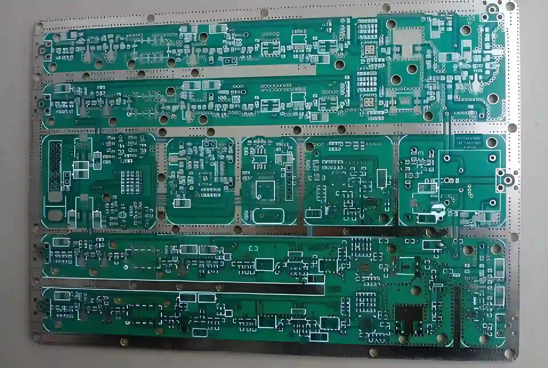
PCB panelization is the process of grouping multiple individual PCB designs onto a single larger panel for manufacturing. Instead of producing each board separately, manufacturers create many boards at once on a shared panel, which is later separated into individual units. This approach offers several benefits, including reduced production costs, faster manufacturing times, and less material waste.
For electrical engineers, understanding panelization is critical because it directly impacts the cost and quality of the final product. Poor panel utilization can lead to wasted materials, higher expenses, and even delays in production due to inefficiencies. On the other hand, a well-optimized panel can lower costs by up to 30% in some cases and improve throughput during assembly. With the right techniques, you can ensure that your designs are not only functional but also cost-effective to produce.
Suggested Image Placement 1
Key Benefits of Optimizing PCB Panel Utilization
Before diving into the how-to, let’s look at why optimizing panel utilization is worth your time and effort. Here are the main advantages:
- Cost Savings: By fitting more boards onto a single panel, you reduce the number of panels needed, cutting down on material and processing costs.
- Reduced Material Waste: Efficient layouts mean less unused space, which minimizes scrap and supports sustainable manufacturing practices.
- Faster Production: Manufacturers can process multiple boards in one go, speeding up fabrication and assembly.
- Improved Handling: Panels are easier to handle during automated assembly compared to individual small boards, reducing the risk of damage.
These benefits are especially important for high-volume production, where even small improvements in efficiency can lead to significant savings. For example, increasing panel utilization from 60% to 80% on a 500-unit order could save hundreds of dollars in material costs alone.
Step 1: Understanding PCB Panel Area Calculation
One of the first steps in maximizing panel utilization is mastering PCB panel area calculation. This involves determining how much usable space is available on a panel and how to arrange your boards to fit as many as possible without violating manufacturing constraints.
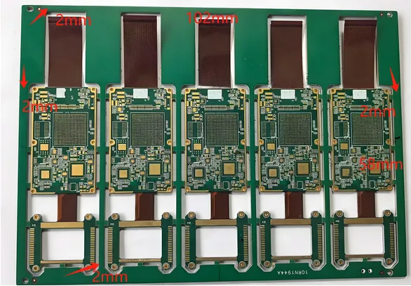
Standard panel sizes vary, but common dimensions include 18 x 24 inches or 12 x 18 inches, depending on the manufacturer. To calculate the usable area, subtract the border margins (typically 0.5 to 1 inch on each side) required for tooling and handling. For an 18 x 24-inch panel with 1-inch margins, the usable area would be 16 x 22 inches, or 352 square inches.
Next, measure the dimensions of your individual PCB design. If your board is 2 x 3 inches (6 square inches), you can theoretically fit about 58 boards on the panel (352 ÷ 6). However, this doesn’t account for spacing between boards, tooling holes, or breakaway tabs. A more realistic estimate, after factoring in a 0.1-inch spacing between boards, might drop this number to around 50 boards per panel.
Using software tools with panelization features can automate these calculations and provide visual layouts to ensure accuracy. The goal is to balance the number of boards with the need for safe spacing and structural integrity during manufacturing.
Suggested Image Placement 2
Step 2: Applying PCB Panelization Optimization Techniques
Once you’ve calculated the panel area, it’s time to apply PCB panelization optimization techniques to make the most of that space. Here are some proven strategies:
1. Use Uniform Board Orientation
Arrange boards in the same orientation whenever possible. Rotating some boards to fit more onto the panel might seem efficient, but it can complicate assembly, especially for automated pick-and-place machines. Uniform orientation reduces setup time and minimizes errors during production.
2. Minimize Spacing Without Compromising Quality
While spacing between boards is necessary for cutting and handling, excessive gaps waste space. Aim for the minimum spacing recommended by your manufacturer, often around 0.08 to 0.12 inches, to fit more boards while ensuring clean separation after fabrication.
3. Consider Mixed Designs on a Single Panel
For projects with multiple board designs, try combining them on the same panel if they share similar manufacturing requirements (e.g., layer count, material, thickness). This reduces the number of separate panels needed and can lower costs, though it requires careful planning to avoid assembly confusion.
4. Optimize for Depanelization Methods
Different separation methods, such as V-scoring or tab-routing, impact how much space you need between boards. V-scoring requires less space (about 0.1 inch) and is ideal for straight cuts, while tab-routing needs more room (0.2 to 0.3 inches) but works for irregular shapes. Choose the method that best fits your design to avoid wasting panel space.
By implementing these techniques, you can increase panel utilization rates significantly. For instance, reducing spacing from 0.2 inches to 0.1 inches on a panel holding 40 boards might allow you to fit an additional 5-10 boards, boosting efficiency by up to 25%.
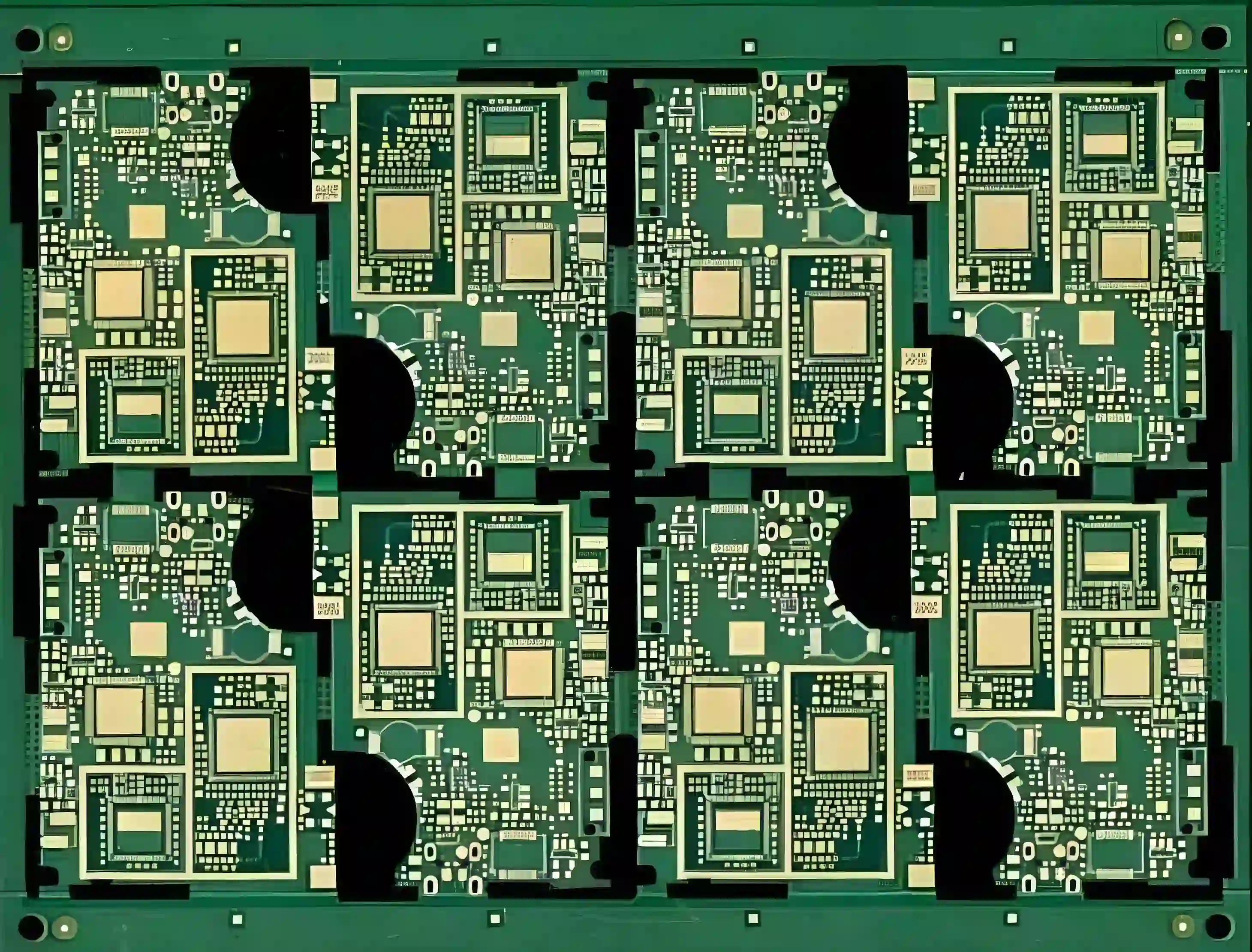
Step 3: Designing an Efficient PCB Layout for Manufacturing
Creating an efficient PCB layout for manufacturing is just as important as panel optimization. A well-thought-out layout ensures that your design fits neatly into the panel while meeting performance and manufacturability requirements. Here are key tips to follow:
1. Keep Components Away from Edges
Place components at least 0.1 to 0.2 inches away from the board edges to prevent damage during depanelization. This buffer zone also helps with handling during assembly and reduces the risk of cracked components.
2. Align with Grid Patterns
Design your board to align with a grid pattern on the panel. This makes it easier to arrange multiple boards systematically, reducing wasted space and simplifying automated assembly processes.
3. Optimize for Signal Integrity
While focusing on layout efficiency, don’t compromise on signal integrity. For high-speed designs, maintain controlled impedance (e.g., 50 ohms for many RF applications) by ensuring consistent trace widths and spacing. Poor layout choices can lead to crosstalk or signal delays, even if the panel utilization is high.
4. Plan for Test Points
Include test points in accessible areas of the board to facilitate in-circuit testing without disrupting the panel layout. This ensures quality control during manufacturing without requiring extra space or rework.
A carefully planned layout not only improves panel utilization but also reduces manufacturing errors, saving time and resources in the long run.
Suggested Image Placement 3
Step 4: Minimizing PCB Material Waste
A major goal of panel optimization is minimizing PCB material waste. Wasted material means higher costs and a larger environmental footprint, so it’s in everyone’s interest to keep scrap to a minimum. Here’s how to achieve that:
1. Use Nesting Software
Specialized software can automatically arrange boards on a panel to minimize unused space. These tools use algorithms to “nest” designs, often achieving utilization rates of 85% or higher, compared to 60-70% with manual layouts.
2. Standardize Board Sizes When Possible
If you’re designing multiple boards for a project, try to standardize their dimensions. Uniform sizes make it easier to fill a panel without awkward gaps, reducing leftover material.
3. Reuse Scrap Material
For smaller projects or prototypes, consider using leftover panel material for test boards or non-critical designs. While this won’t work for high-volume production, it’s a practical way to repurpose waste in smaller runs.
By focusing on these strategies, you can cut material waste by 10-20% on average, depending on the complexity of your design and the tools you use.
Step 5: Following PCB Panel Design Rules
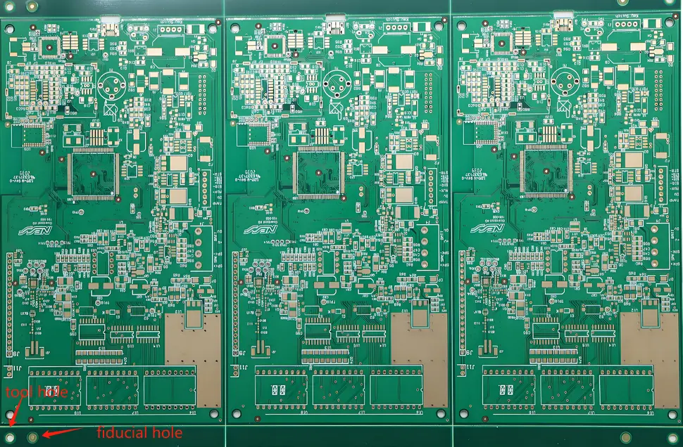
Lastly, adhering to PCB panel design rules is essential for ensuring that your optimized panel can be manufactured without issues. These rules are often provided by manufacturers and cover aspects like spacing, tooling, and panel strength. Here are some common guidelines:
- Tooling Holes: Include non-plated tooling holes (typically 0.125 inches in diameter) in the panel margins for alignment during fabrication. Place them at least 0.5 inches from the panel edge.
- Breakaway Tabs: If using tab-routing for depanelization, design tabs with a width of 0.2 to 0.3 inches and include perforations to make separation easier without damaging boards.
- Panel Strength: Ensure the panel has enough structural integrity by avoiding overly thin borders or excessive cutouts that could cause it to warp or break during processing.
- Fiducial Marks: Add fiducial marks (small copper circles) on the panel for alignment during automated assembly. Place at least three marks per panel, ideally near the corners.
Following these rules prevents costly manufacturing errors and ensures that your optimized panel design translates into a high-quality final product.
Common Challenges in PCB Panel Utilization and How to Overcome Them
Even with the best planning, challenges can arise during panel optimization. Here are a few common issues and solutions:
- Irregular Board Shapes: Non-rectangular boards can create gaps on the panel. Use nesting software or filler designs (like dummy boards) to fill unused space.
- High Component Density: Boards with tall or dense components may require extra spacing to avoid interference during assembly. Plan for this early in the layout stage by consulting with your manufacturer.
- Thermal Stress: Uneven copper distribution across a panel can cause warping during soldering. Balance copper layers and add dummy fills if needed to distribute heat evenly.
Addressing these challenges upfront saves time and prevents costly redesigns later in the process.
Conclusion: Take Control of Your PCB Panel Utilization
Maximizing PCB panel utilization is a powerful way for electrical engineers to enhance efficiency, reduce costs, and support sustainable manufacturing practices. By mastering PCB panelization optimization techniques, performing accurate PCB panel area calculation, designing an efficient PCB layout for manufacturing, focusing on minimizing PCB material waste, and adhering to PCB panel design rules, you can transform your designs into cost-effective, high-quality products.
Start by analyzing your current panel layouts and identifying areas for improvement. Use the strategies outlined in this guide to refine your approach, and leverage software tools to automate and perfect the process. With practice and attention to detail, you’ll be able to achieve panel utilization rates that benefit both your bottom line and your project timelines. Take the first step today and see the difference optimization can make in your next PCB project.


