 ALLPCB


If you're designing a printed circuit board (PCB) and need to understand how to connect layers effectively, through-hole vias are a fundamental solution. These tiny drilled holes, plated with conductive material, create electrical connections between different layers in a multilayer PCB. In this comprehensive guide, we'll explore everything you need to know about through-hole via types, PCB layer stackup, via connections, multilayer PCB design, and via design rules to ensure your boards are reliable and efficient.
Whether you're a beginner or an experienced engineer, this blog will walk you through the essentials and advanced tips for mastering through-hole vias. Let's dive into the details of how these components work and how to use them effectively in your designs.
What Are Through-Hole Vias and Why Are They Important?
Through-hole vias are small holes drilled through a PCB that extend from the top layer to the bottom layer, passing through all intermediate layers. These holes are then plated with a conductive material, usually copper, to create an electrical connection between layers. They are a cornerstone of multilayer PCB designs, enabling complex circuits to fit into smaller spaces by stacking conductive layers.
The importance of through-hole vias lies in their ability to simplify routing in dense designs. Without vias, signals and power would be limited to a single layer, making it nearly impossible to create compact, high-performance electronics like smartphones or medical devices. By using through-hole vias, you can connect traces across multiple layers, optimize space, and improve signal integrity.
Key Benefits of Through-Hole Vias
- Space Efficiency: They allow for vertical connections, freeing up surface area for components.
- Signal Integrity: Properly designed vias reduce signal loss and interference.
- Power Distribution: They help distribute power and ground across layers, reducing noise.
Types of Through-Hole Vias in PCB Design
Understanding the different through-hole via types is crucial for selecting the right one for your design. Each type serves a specific purpose based on the PCB's complexity and manufacturing constraints. Below are the primary categories of through-hole vias commonly used in multilayer PCBs.
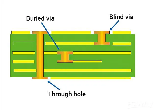
1. Standard Through-Hole Vias
These are the most common type, extending through all layers of the PCB. They are used for basic interlayer connections and are cost-effective for most designs. Standard vias are ideal for low-density boards where space isn’t a critical constraint.
2. Blind Vias
Blind vias start from an outer layer (top or bottom) and connect to an inner layer without passing through the entire board. They are useful in high-density interconnect (HDI) designs as they save space on the opposite side of the board. However, they are more expensive to manufacture due to the precision required.
3. Buried Vias
Buried vias connect internal layers without reaching the outer surfaces of the PCB. They are invisible from the outside and are often used in very complex multilayer designs to maximize surface space for components. Like blind vias, they increase manufacturing costs but are essential for advanced applications.
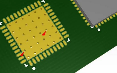
4. Thermal Vias
Thermal vias are designed to dissipate heat from components like power ICs to a heat sink or ground plane. They are typically arranged in an array under a component to transfer heat efficiently. For example, a thermal via array under a high-power LED might use 0.3mm diameter vias spaced 1mm apart to manage heat effectively.
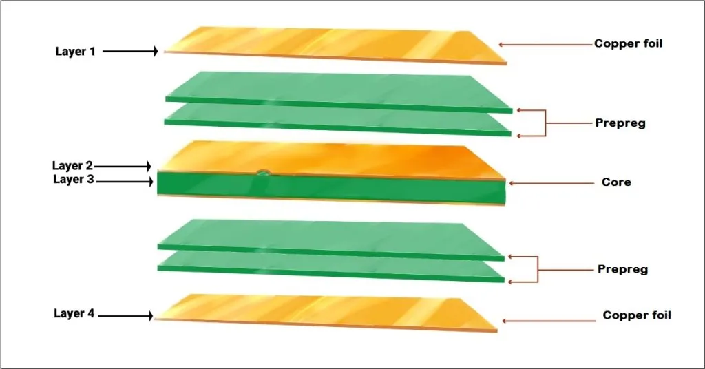
Understanding PCB Layer Stackup and Via Connections
PCB layer stackup refers to the arrangement of conductive copper layers and insulating materials in a multilayer PCB. A well-planned stackup is essential for signal integrity, power distribution, and manufacturability. Through-hole vias play a critical role in connecting these layers, and their placement must align with the stackup design.
Basics of PCB Layer Stackup
A typical 4-layer PCB stackup might include:
- Top Layer (Signal): For component placement and routing.
- Ground Plane: Reduces noise and provides a return path for signals.
- Power Plane: Distributes power to components.
- Bottom Layer (Signal): Additional routing and components.
In an 8-layer PCB, additional signal and plane layers are added for more complex routing. The dielectric thickness between layers (often 0.1mm to 0.2mm for high-speed designs) impacts impedance, which must be controlled for signals operating at frequencies above 100 MHz.
How Vias Fit into Stackup Design
Through-hole vias connect these layers vertically. For instance, a standard via might connect a signal from the top layer to the bottom layer, passing through ground and power planes. However, vias that pass through power or ground planes can create unwanted capacitance or inductance, affecting signal speeds. To mitigate this, designers often place vias close to decoupling capacitors or use stitching vias to connect ground planes, reducing loop inductance to below 1 nH.
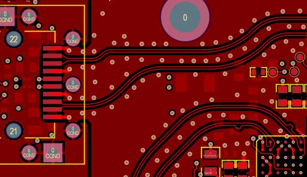
Via Connections in Multilayer PCB Design
In multilayer PCBs, via connections are more than just holes—they are critical pathways for signals, power, and ground. Poorly designed vias can lead to signal degradation, increased noise, or even board failure. Here’s how to approach via connections in multilayer designs.
Signal Vias
Signal vias carry data between layers. For high-speed signals (above 1 GHz), the via’s length and diameter impact impedance. A via with a diameter of 0.25mm and a length of 1.6mm (standard for a 4-layer board) might introduce a parasitic capacitance of around 0.5 pF, which can distort signals. To minimize this, use smaller vias or add ground vias nearby to create a controlled impedance path.
Power and Ground Vias
Power and ground vias connect to internal planes to ensure stable voltage levels across the board. Multiple vias (e.g., 4-6 vias per power pin for high-current ICs) are often used to reduce resistance and inductance. For a 3A current path, using vias with a 0.3mm diameter can handle the load without overheating if spaced properly.
Via Stitching
Via stitching involves placing multiple vias to connect ground planes across layers, reducing electromagnetic interference (EMI). For example, placing ground vias every 5mm along the board edge can create a "fence" to contain high-frequency noise above 500 MHz.
Via Design Rules for Optimal PCB Performance
To ensure reliability and manufacturability, following via design rules is essential. These guidelines help balance performance with cost and prevent issues like signal loss or drilling errors during production.
1. Via Size and Aspect Ratio
The diameter and depth of a via affect its manufacturability. A common rule is to keep the aspect ratio (depth-to-diameter) below 10:1 for standard through-hole vias. For a 1.6mm thick board, a via diameter of 0.2mm or larger is recommended. Smaller vias (e.g., 0.1mm) are possible but increase costs and require advanced drilling techniques.
2. Via Spacing
Vias should be spaced at least 0.5mm apart (center-to-center) to avoid structural weaknesses in the PCB. For high-density designs, consult your manufacturer for tighter spacing limits, as drilling precision varies.
3. Annular Ring Requirements
The annular ring is the copper pad surrounding a via. A minimum width of 0.15mm per side ensures a reliable connection after drilling. For a 0.3mm via, the pad diameter should be at least 0.6mm to account for manufacturing tolerances.
4. Via Placement Near Components
Avoid placing vias under surface-mount components unless necessary, as they can interfere with soldering. If unavoidable, use tented vias (covered with solder mask) to prevent solder wicking, especially for vias smaller than 0.4mm in diameter.
5. Thermal Via Design
For thermal vias, use an array with a pitch of 1.0mm to 1.2mm to maximize heat transfer without weakening the board. Ensure the vias are connected to a large copper plane for effective heat dissipation.
Challenges and Solutions in Through-Hole Via Design
Designing with through-hole vias isn’t without challenges. Here are some common issues and how to address them in multilayer PCB projects.
Challenge 1: Signal Integrity Issues
Long vias in high-speed designs can act as stubs, causing reflections. For signals above 2 GHz, a via stub might resonate and degrade the signal. Solution: Use back-drilling to remove unused portions of the via, reducing stub length to under 0.2mm.
Challenge 2: Manufacturing Limitations
Small vias or high aspect ratios can lead to drilling errors or plating defects. Solution: Stick to manufacturer guidelines, typically recommending via diameters no smaller than 0.2mm for cost-effective production.
Challenge 3: Thermal Management
Inadequate thermal vias can cause overheating in power-intensive designs. Solution: Calculate the required number of thermal vias based on current and heat dissipation needs. For a 5W component, an array of 10-15 thermal vias might be necessary.
Best Practices for Through-Hole Via Implementation
To wrap up, here are some actionable best practices for incorporating through-hole vias into your PCB designs:
- Plan your layer stackup early to determine via placement and type.
- Use simulation tools to analyze signal integrity for high-speed designs, targeting impedance values around 50 ohms for most digital signals.
- Collaborate with your PCB manufacturer to confirm via size and spacing capabilities before finalizing the design.
- Minimize via count where possible to reduce costs, but don’t compromise on power or ground connections.
- Document via usage (e.g., signal, power, thermal) in your design files for clarity during assembly.
Conclusion: Elevate Your PCB Designs with Through-Hole Vias
Mastering through-hole vias is a key skill for any PCB designer working on multilayer boards. By understanding the different through-hole via types, optimizing PCB layer stackup, ensuring reliable via connections, and following via design rules, you can create boards that are both high-performing and cost-effective. These small but mighty components are the backbone of complex electronics, enabling everything from consumer gadgets to industrial systems.
As you apply these principles to your next project, remember that attention to detail in via design can make a significant difference in signal quality and board reliability. With the right approach, through-hole vias will help you achieve compact, efficient, and robust PCB designs tailored to your needs.


