 ALLPCB


If you're looking to design a PCB with precise 50 ohm impedance control, you've come to the right place. Achieving 50 ohm impedance in your PCB stackup is critical for high-frequency and RF applications to ensure signal integrity and minimize losses. In this guide, we'll walk you through the essentials of designing a 50 ohm impedance PCB stackup, including microstrip impedance calculation, stripline impedance design, PCB material selection for 50 ohm, and tips for impedance control layer stack planning. Whether you're an experienced engineer or just starting with RF designs, this comprehensive resource will help you master the process with actionable steps and practical insights.
Why 50 Ohm Impedance Matters in PCB Design
In high-frequency and radio frequency (RF) applications, maintaining a specific impedance—often 50 ohms—is vital for optimal signal transmission. The 50 ohm standard is widely used in RF systems because it provides a good balance between power handling and signal loss, making it ideal for antennas, amplifiers, and other communication devices. Without proper impedance control, you risk signal reflections, power loss, and degraded performance in your circuit.
Designing a PCB stackup for 50 ohm impedance involves carefully selecting materials, calculating trace dimensions, and arranging layers to match the desired impedance. Let’s dive into the key aspects of this process to help you achieve reliable and efficient designs.
Understanding the Basics of 50 Ohm Impedance in PCBs
Impedance in a PCB refers to the resistance to the flow of alternating current (AC) signals along a trace. For RF signals, a consistent 50 ohm impedance ensures that the signal travels from source to load without significant reflections. Mismatched impedance can cause standing waves, leading to energy loss and poor system performance.
There are two primary transmission line structures used in PCBs to achieve 50 ohm impedance: microstrip and stripline. Microstrip traces are placed on the outer layers of the PCB with a ground plane beneath, while stripline traces are sandwiched between two ground planes within internal layers. Each structure has unique characteristics and design considerations, which we'll explore in detail.
Key Factors in 50 Ohm Impedance PCB Stackup Design
Creating a PCB stackup for 50 ohm impedance requires attention to several factors, including layer arrangement, trace geometry, and material properties. Below, we break down the critical elements to consider during the design process.
1. Layer Stackup Configuration
The layer stackup defines how many layers your PCB will have and how they are arranged. For 50 ohm impedance control, a multilayer PCB (typically 4 or more layers) is common, as it allows for dedicated ground planes and controlled trace placement. A typical 4-layer stackup might look like this:
- Top Layer: Signal (Microstrip traces)
- Layer 2: Ground Plane
- Layer 3: Power Plane
- Bottom Layer: Signal or Ground
The ground plane directly beneath a microstrip trace or surrounding a stripline trace plays a crucial role in determining impedance. Keeping the dielectric thickness consistent between the signal layer and ground plane is essential for maintaining uniform impedance across the board.
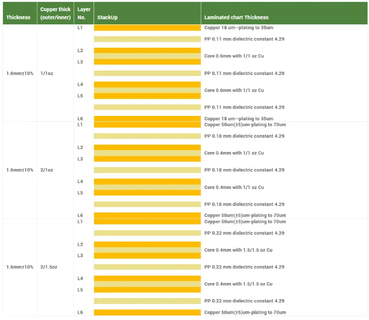
2. Dielectric Constant (Dk) and Material Selection
The dielectric material between layers affects the signal speed and impedance. The dielectric constant (Dk) of the material influences how much the signal is slowed down as it travels through the PCB. For 50 ohm impedance designs, materials with a stable Dk value (typically between 3.5 and 4.5) are preferred. Common materials include FR-4 for cost-effective designs and high-frequency laminates like Rogers or Isola for superior performance in RF applications.
When selecting a PCB material for 50 ohm impedance, consider the following:
- Low Loss Tangent: Materials with a low loss tangent reduce signal attenuation at high frequencies.
- Thermal Stability: Ensure the material maintains its properties under varying temperatures.
- Cost vs. Performance: Balance the need for high-performance materials with budget constraints.
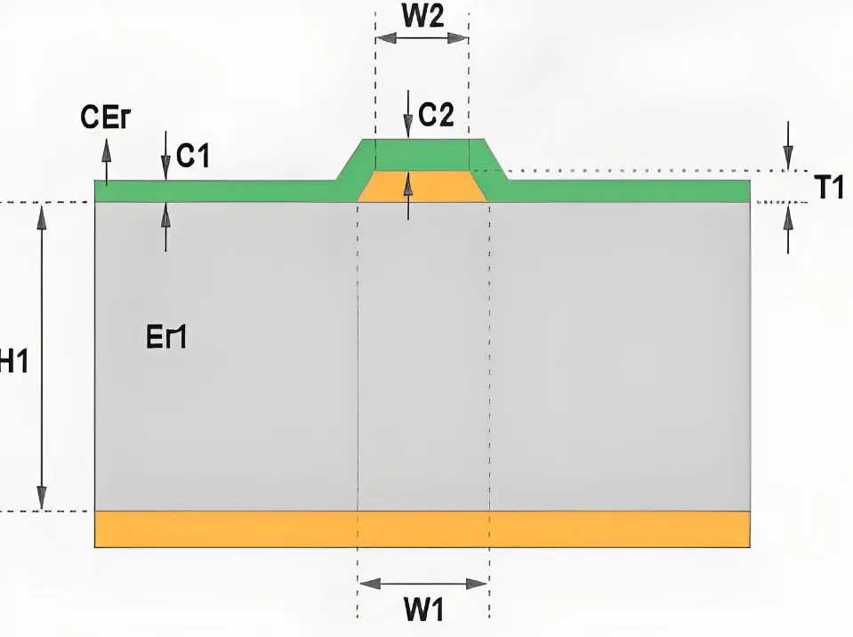
3. Trace Width and Spacing
The width of the trace and its distance from the ground plane directly impact the impedance. For a microstrip line, a wider trace results in lower impedance, while a narrower trace increases it. Similarly, the dielectric thickness between the trace and ground plane affects the impedance value. For stripline designs, the trace is sandwiched between two ground planes, and the spacing between these planes must be carefully controlled.
As a rule of thumb, for a standard 4-layer PCB with FR-4 material (Dk ≈ 4.2), a trace width of approximately 6-8 mils and a dielectric thickness of 5-6 mils can achieve 50 ohm impedance for microstrip lines. However, these values vary based on material properties and stackup configuration, so precise calculations are necessary.
Related Reading: How PCB Trace Width Affects Impedance: A Practical Guide
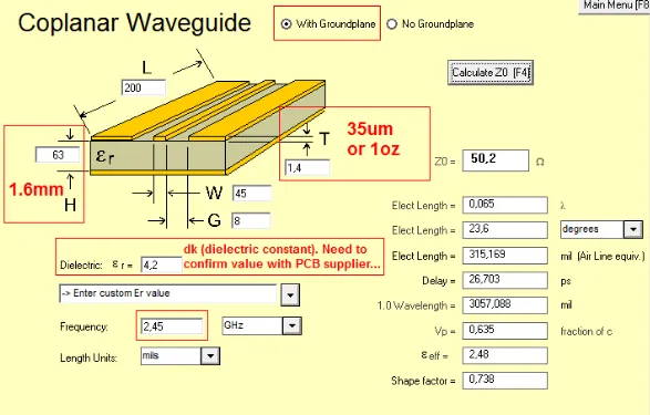
Microstrip Impedance Calculation for 50 Ohm Design
Calculating the impedance of a microstrip trace is a critical step in achieving 50 ohm impedance. The impedance depends on the trace width (W), dielectric thickness (H), and dielectric constant (Dk) of the substrate. The following simplified formula is often used for microstrip impedance calculation:
Z? ≈ (87 / √(Dk + 1.41)) * ln(5.98 * H / (0.8 * W + T))
Where:
- Z? = Characteristic impedance (ohms)
- H = Dielectric thickness (mils)
- W = Trace width (mils)
- T = Trace thickness (mils)
- Dk = Dielectric constant of the material
For a practical example, consider a PCB with a dielectric thickness of 6 mils, a trace thickness of 1.4 mils, and a Dk of 4.2. To achieve 50 ohm impedance, you would adjust the trace width to approximately 7 mils. However, manual calculations can be tedious and prone to error. Using simulation tools or online calculators can simplify this process and provide more accurate results tailored to your specific stackup.
Related Reading: Understanding Impedance Calculators: Optimizing Signal Integrity in PCB Design
Stripline Impedance Design for 50 Ohm Control
Stripline designs are often used when better shielding and lower crosstalk are needed compared to microstrip. In a stripline configuration, the trace is embedded between two ground planes, and the impedance depends on the trace width (W), the distance between the ground planes (B), and the dielectric constant (Dk). A simplified formula for stripline impedance is:
Z? ≈ (60 / √Dk) * ln(4 * B / (0.67 * π * (0.8 * W + T)))
Where:
- Z? = Characteristic impedance (ohms)
- B = Distance between ground planes (mils)
- W = Trace width (mils)
- T = Trace thickness (mils)
- Dk = Dielectric constant
For a 50 ohm stripline in a multilayer PCB with a Dk of 4.2 and a ground plane spacing of 10 mils, the trace width might be around 4-5 mils. Stripline designs are more complex to fabricate due to their internal placement, but they offer better signal integrity for high-frequency applications.
PCB Material Selection for 50 Ohm Impedance
Choosing the right material is a cornerstone of achieving 50 ohm impedance in your PCB design. The material’s dielectric constant (Dk) and loss tangent directly influence signal propagation and loss. Here are some tips for effective material selection:
- Standard FR-4: Suitable for lower-frequency designs (up to a few GHz) with a Dk of around 4.2-4.5. It’s cost-effective but may not perform well at very high frequencies due to higher losses.
- High-Frequency Laminates: Materials like Rogers 4350B or Isola IS620 offer lower Dk values (around 3.5-3.7) and lower loss tangents, making them ideal for RF designs above 5 GHz.
- Consistency: Ensure the material has uniform Dk across the board to avoid impedance variations.
Work closely with your PCB manufacturer to confirm material availability and stackup compatibility. Providing detailed specifications for dielectric thickness and material type ensures that your design meets the 50 ohm impedance target.
Best Practices for Impedance Control Layer Stack Design
Designing an impedance control layer stack requires a systematic approach to ensure consistency and performance. Follow these best practices to optimize your 50 ohm impedance PCB stackup:
- Maintain Symmetry: A symmetrical stackup reduces the risk of warping during manufacturing and ensures uniform thermal expansion.
- Dedicated Ground Planes: Place ground planes adjacent to signal layers to provide a consistent reference for impedance control.
- Minimize Via Transitions: Vias can introduce impedance discontinuities. Use back-drilling or blind vias for high-frequency signals to reduce stub effects.
- Simulate and Test: Use simulation software to model your stackup and verify impedance values before fabrication. Post-fabrication testing with a Time Domain Reflectometer (TDR) can confirm the results.
Common Challenges in 50 Ohm Impedance Design and How to Overcome Them
Designing for 50 ohm impedance is not without challenges. Here are some common issues and solutions:
- Material Variations: Dielectric constants can vary between batches. Specify tight tolerances with your manufacturer to minimize deviations.
- Trace Etching Accuracy: Over- or under-etching can alter trace widths. Include test coupons on your PCB to verify trace dimensions after fabrication.
- High-Frequency Losses: At frequencies above 10 GHz, signal losses become significant. Opt for low-loss materials and keep trace lengths short.
Tools and Resources for 50 Ohm Impedance Design
Several tools can simplify the process of designing a 50 ohm impedance PCB stackup. Simulation software like Altium Designer or Cadence Allegro offers built-in impedance calculators and stackup planners. Additionally, free online tools are available for quick microstrip and stripline impedance calculations. These tools allow you to input your material properties and layer dimensions to get accurate trace width recommendations.
Collaborating with your PCB manufacturer early in the design phase is also beneficial. They can provide stackup recommendations, material datasheets, and feedback on manufacturability to ensure your design achieves the desired impedance.
Conclusion: Achieving Precision with 50 Ohm Impedance Control
Mastering stackup design for 50 ohm impedance control is a critical skill for engineers working on high-frequency and RF applications. By understanding the fundamentals of microstrip impedance calculation, stripline impedance design, and PCB material selection for 50 ohm, you can create reliable and efficient designs that meet stringent performance requirements. A well-planned impedance control layer stack, combined with accurate calculations and the right materials, ensures signal integrity and minimizes losses in your circuits.
Start by defining your stackup configuration, selecting appropriate materials, and using simulation tools to verify your design. With attention to detail and adherence to best practices, you’ll be well-equipped to tackle the challenges of 50 ohm impedance PCB design. Trust in the process, collaborate with your manufacturing partner, and leverage the insights from this guide to elevate your next project.


