 ALLPCB


If you're looking to design a high-performing RF PCB with excellent signal integrity, mastering the stack-up is key. A well-planned RF PCB stack-up ensures minimal signal loss, controlled impedance, and reduced electromagnetic interference (EMI). In this guide, we'll dive deep into the essentials of RF PCB stackup design, covering layer arrangement, impedance control, EMI reduction, and material selection to help you achieve optimal performance for your high-frequency applications.
Whether you're an experienced engineer or just starting with RF designs, this comprehensive guide will walk you through practical strategies and actionable tips. Let’s explore how to build an effective RF PCB layer arrangement that meets the demands of modern electronics.
Why RF PCB Stack-Up Matters for Signal Integrity
RF (Radio Frequency) PCBs operate at high frequencies, often in the range of hundreds of megahertz to several gigahertz. At these frequencies, even small design flaws can lead to significant signal degradation, crosstalk, or EMI issues. The stack-up—the arrangement of layers in a PCB—plays a critical role in maintaining signal integrity by providing a stable environment for signal transmission.
A proper RF PCB stackup design addresses challenges like impedance mismatches (which can cause signal reflections) and EMI (which can interfere with nearby circuits). For example, a poorly designed stack-up might result in a 50-ohm trace deviating to 60 ohms due to inconsistent dielectric thickness, leading to up to 20% signal reflection. By optimizing the stack-up, you ensure consistent performance, lower noise, and better overall functionality for applications like wireless communication, radar systems, and IoT devices.
Key Elements of RF PCB Stack-Up Design
Designing an effective stack-up for RF applications involves several critical factors. Below, we break down the essential components to focus on during the design process.
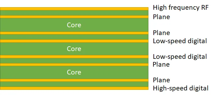
1. Understanding RF PCB Layer Arrangement
The RF PCB layer arrangement determines how signals, power, and ground planes are positioned within the board. A typical RF PCB might use a 4-layer or 6-layer stack-up, though more complex designs can go up to 8 or 10 layers. Here’s a common 4-layer stack-up for RF applications:
- Top Layer: RF signal traces and components.
- Layer 2: Ground plane for signal return paths and shielding.
- Layer 3: Power plane or additional ground for isolation.
- Bottom Layer: Additional signal traces or ground.
In high-frequency designs, placing a ground plane directly beneath the signal layer minimizes loop inductance and ensures a consistent return path. For instance, separating signal layers with a ground plane can reduce crosstalk by up to 30% in designs operating at 2.4 GHz, a common frequency for Wi-Fi applications.
Keep layer thickness consistent to maintain uniform impedance. Variations as small as 0.1 mm in dielectric thickness can alter impedance by 5-10 ohms, disrupting signal integrity. Symmetry in the stack-up also prevents warping during manufacturing, ensuring long-term reliability.
2. RF PCB Stack-Up Impedance Control
Impedance control is a cornerstone of RF PCB stackup impedance control. RF signals require a specific characteristic impedance—often 50 ohms for most RF systems—to prevent signal reflections and ensure maximum power transfer. Achieving this requires careful calculation of trace width, dielectric thickness, and material properties.
For example, in a microstrip configuration (a common RF trace design), a 50-ohm impedance on a standard 1.6 mm thick board with a dielectric constant of 4.4 (like FR-4) might require a trace width of approximately 2.8 mm. However, at higher frequencies above 1 GHz, FR-4 can introduce significant signal loss due to its high dissipation factor. Adjusting the stack-up by using thinner dielectric layers or low-loss materials can help maintain the desired impedance.
Use simulation tools to model impedance before fabrication. Even a 5% deviation from the target impedance can lead to noticeable signal degradation in systems operating at 5 GHz or higher. Additionally, ensure that vias and transitions between layers don’t disrupt impedance, as discontinuities can cause reflections.
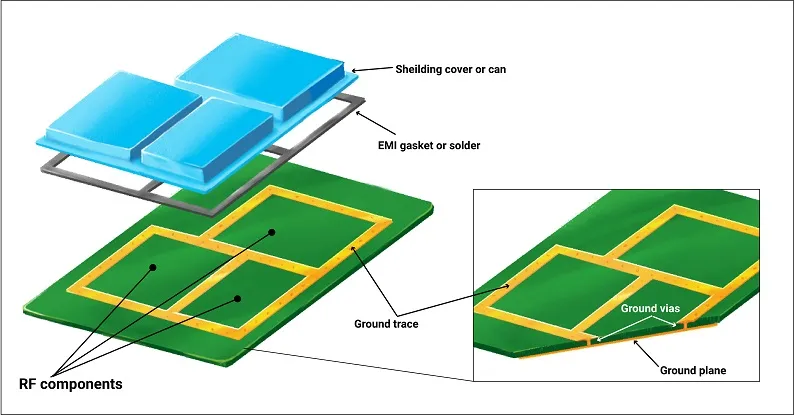
3. RF PCB Stack-Up EMI Reduction
Electromagnetic interference (EMI) is a major concern in RF designs, as high-frequency signals can easily radiate energy or pick up noise from nearby circuits. Effective RF PCB stackup EMI reduction starts with proper layer planning and shielding.
Place ground planes adjacent to signal layers to create a low-impedance return path and contain electromagnetic fields. For instance, a continuous ground plane can reduce EMI by up to 40% compared to a split or incomplete plane. Avoid routing high-speed signals over split planes, as this can create large current loops and increase radiation.
In a 6-layer stack-up, you might dedicate two internal layers to ground planes, sandwiching signal layers to provide shielding on both sides. This approach is particularly effective for designs operating above 1 GHz, where EMI can degrade performance by introducing noise levels as high as 10-15 dB above the desired signal.
Additionally, keep power and ground planes close together to form a decoupling capacitor effect, reducing noise in the power distribution network. A separation of 0.1 mm between power and ground layers can lower power supply noise by up to 20% in high-frequency designs.
4. RF PCB Stack-Up Material Selection
Material choice is a critical aspect of RF PCB stackup material selection. The dielectric material between layers affects signal speed, loss, and impedance. At RF frequencies, standard materials like FR-4 may not suffice due to their higher dielectric constant (around 4.4) and dissipation factor (around 0.02), which cause signal attenuation above 1 GHz.
For better performance, consider low-loss materials with dielectric constants between 2.2 and 3.5 and dissipation factors below 0.005. These materials minimize signal loss and maintain stable impedance at frequencies up to 10 GHz or higher. However, they can be more expensive, so balance cost with performance needs based on your application.
The thickness of the dielectric also matters. Thinner dielectrics (e.g., 0.2 mm) allow for tighter impedance control but may increase manufacturing costs. Thicker dielectrics (e.g., 0.8 mm) are cheaper but can make it harder to achieve precise impedance in compact designs. Work with your fabrication partner to select a material and thickness that aligns with your frequency range and budget.
Best Practices for Designing an RF PCB Stack-Up
Now that we’ve covered the core elements, let’s look at some actionable best practices to ensure your RF PCB stack-up supports signal integrity.
- Prioritize Symmetry: Design a symmetrical stack-up to prevent board warping. For example, in a 6-layer board, balance the number of dielectric layers and copper weights on both sides of the center.
- Minimize Via Transitions: Each via introduces impedance discontinuities. Use back-drilling or blind vias to reduce stub effects, especially in designs above 3 GHz, where stub resonance can degrade signals by 10-15%.
- Optimize Trace Routing: Keep RF traces short and direct. Avoid sharp 90-degree bends; use 45-degree angles or curved traces to prevent signal reflections, which can increase loss by up to 5% per bend at 5 GHz.
- Simulate and Test: Use electromagnetic simulation software to model your stack-up before fabrication. Test prototypes with a vector network analyzer to verify impedance and signal integrity, ensuring performance matches design expectations.
Common Challenges and How to Overcome Them
Designing an RF PCB stack-up isn’t without challenges. Here are a few common issues and solutions:
Challenge 1: Signal Loss at High Frequencies
Signal loss increases with frequency due to dielectric and conductor losses. To mitigate this, select low-loss materials and use wider traces where possible to reduce skin effect losses. For a 10 GHz signal, switching to a material with a dissipation factor of 0.002 can reduce loss by up to 25% compared to standard materials.
Challenge 2: Manufacturing Tolerances
Variations in layer thickness or copper etching during fabrication can affect impedance. Specify tight tolerances (e.g., ±0.05 mm for dielectric thickness) in your design files and collaborate closely with your manufacturer to ensure consistency.
Challenge 3: Cost Constraints
High-performance materials and complex stack-ups can drive up costs. Focus on optimizing only the critical layers (e.g., signal and adjacent ground) with premium materials, while using cost-effective options for less sensitive layers.
Conclusion: Building Better RF PCBs with Optimized Stack-Ups
Mastering RF PCB stackup design is essential for achieving superior signal integrity in high-frequency applications. By focusing on proper RF PCB layer arrangement, implementing RF PCB stackup impedance control, ensuring RF PCB stackup EMI reduction, and making informed RF PCB stackup material selection, you can create designs that perform reliably even under demanding conditions.
Remember to simulate your designs, test prototypes, and work closely with your fabrication partner to address manufacturing constraints. With these strategies, you’ll be well-equipped to tackle the challenges of RF PCB design and deliver high-quality solutions for wireless, radar, and other cutting-edge technologies.
Start applying these principles to your next project and see the difference a well-designed stack-up can make in maintaining signal integrity and overall performance.


