 ALLPCB


If you're a PCB design engineer looking to streamline production and reduce costs, mastering multi-board panelization is a game-changer. In this guide, we'll dive into the essentials of PCB panelization, offering a step-by-step tutorial, multi-board design guidelines, and best practices for design for manufacturability. Whether you're new to panelization or seeking to optimize your process, this comprehensive resource will equip you with the tools and knowledge to create efficient, high-quality PCB panels.
What Is PCB Panelization and Why Does It Matter?
PCB panelization is the process of grouping multiple printed circuit boards (PCBs) into a single panel or array for manufacturing. This technique is widely used to improve production efficiency, minimize material waste, and reduce costs during fabrication and assembly. By arranging several smaller boards on one panel, manufacturers can process them simultaneously, saving time and resources.
For design engineers, panelization is critical because it directly impacts the manufacturability of your designs. A well-panelized layout ensures smoother production runs, fewer errors, and better yields. Poor panelization, on the other hand, can lead to issues like board damage during depanelization, misalignment, or increased costs due to wasted materials. In this guide, we'll explore how to master multi-board panelization to achieve optimal results.
Understanding the Basics of a PCB Panelization Tutorial
Before diving into complex multi-board designs, let’s cover the fundamental steps of panelization. This tutorial is designed to help engineers new to the concept get started with confidence.
- Determine Board Dimensions and Spacing: Measure the size of each individual PCB and decide on the spacing between them. A common spacing is 2-3 mm to allow for breakaway tabs or scoring lines. Ensure the total panel size fits within the manufacturer’s standard panel dimensions, often 18x24 inches or 12x18 inches.
- Choose a Panelization Method: Select between V-Cut scoring (ideal for straight edges) or tab routing (better for irregular shapes). V-Cut uses a scoring wheel to create a groove for easy separation, while tab routing involves milling small tabs that can be broken off post-assembly.
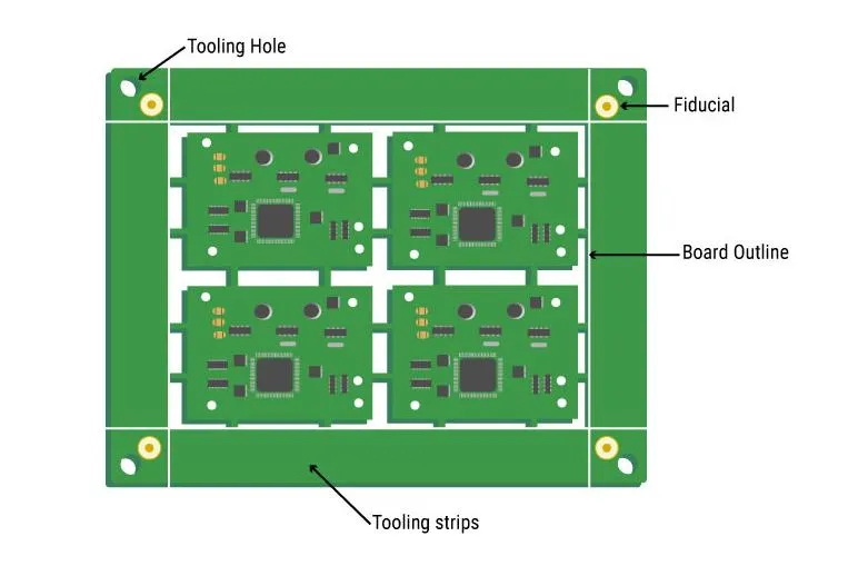
- Add Fiducials and Tooling Holes: Include fiducial marks (typically 1 mm in diameter) on the panel for alignment during assembly. Tooling holes (usually 3-4 mm) help secure the panel during manufacturing.
- Check Design Rules: Verify that your panel layout complies with the manufacturer’s design rules, such as minimum border width (often 5-10 mm) and clearance around components near panel edges.
- Export Panel Files: Generate Gerber files or other required formats for the entire panel, not just individual boards, to ensure the manufacturer receives the correct layout.
Following these steps will help you create a functional panel layout that minimizes errors during production. As you gain experience, you can adapt these basics to more complex multi-board designs.
Multi-Board Design Guidelines for Effective Panelization
Designing multiple boards for panelization requires careful planning to ensure compatibility and efficiency. These multi-board design guidelines will help you create layouts that are easy to manufacture and assemble.
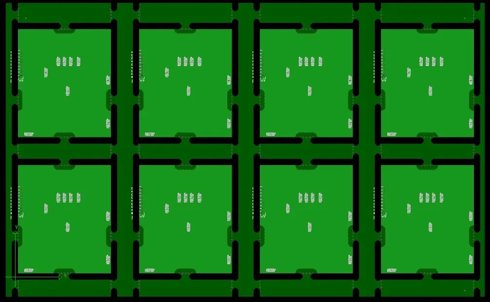
- Uniform Board Sizes When Possible: If your project involves multiple identical boards, arrange them in a consistent grid pattern to simplify panelization. For example, a panel of 10 identical 50x50 mm boards can be arranged in a 2x5 grid with 3 mm spacing, fitting neatly into a standard panel size.
- Mix Board Sizes Strategically: When working with different board sizes, group similar sizes together to maximize panel space. Place larger boards in the center and smaller ones along the edges to balance the panel and reduce stress during depanelization.
- Consider Component Placement: Avoid placing tall or sensitive components (like connectors or capacitors over 5 mm in height) near the edges of individual boards. This prevents damage during separation. Maintain a clearance of at least 2 mm from the board edge for such components.
- Account for Depanelization Stress: Depanelization can cause mechanical stress, especially with V-Cut methods. For delicate designs, opt for tab routing with breakaway tabs (typically 0.5-1 mm thick) to minimize stress on components.
- Rotate Boards for Efficiency: If your boards have an irregular shape, rotating them by 90 or 180 degrees can often improve panel space usage. Use design software to test different orientations before finalizing the layout.
By adhering to these guidelines, you can create multi-board panels that optimize space, reduce waste, and ensure a smooth manufacturing process.
Panelization Best Practices for Design Engineers
To take your panelization skills to the next level, incorporate these panelization best practices into your workflow. These tips focus on achieving high-quality results while maintaining cost-effectiveness.
- Communicate with Manufacturers Early: Before finalizing your panel design, share a draft with your manufacturing partner. They can provide feedback on panel size constraints, preferred depanelization methods, and other specifications that affect production.
- Use Breakaway Tabs for Flexibility: For panels with irregular board shapes, design breakaway tabs with perforations (often 5-7 small holes spaced 0.3 mm apart). This makes separation easier and reduces the risk of board damage.
- Minimize Material Waste: Arrange boards to use as much of the panel area as possible. For instance, if a standard panel is 18x24 inches, aim to fill at least 80-90% of the space to keep costs down.
- Include Test Coupons: Add test coupons (small strips of PCB material) on the panel edges to verify manufacturing quality. These can include traces with specific widths (e.g., 0.2 mm) to test etching accuracy or vias to check drilling precision.
- Balance Panel Strength: Ensure the panel has enough structural integrity during assembly by avoiding overly thin borders (less than 5 mm) or excessive cutouts that weaken the panel.
Implementing these best practices can significantly improve the outcome of your panelization efforts, leading to higher yields and fewer production issues.
Suggested Image Placement 4
Location: After the "Panelization Best Practices" section
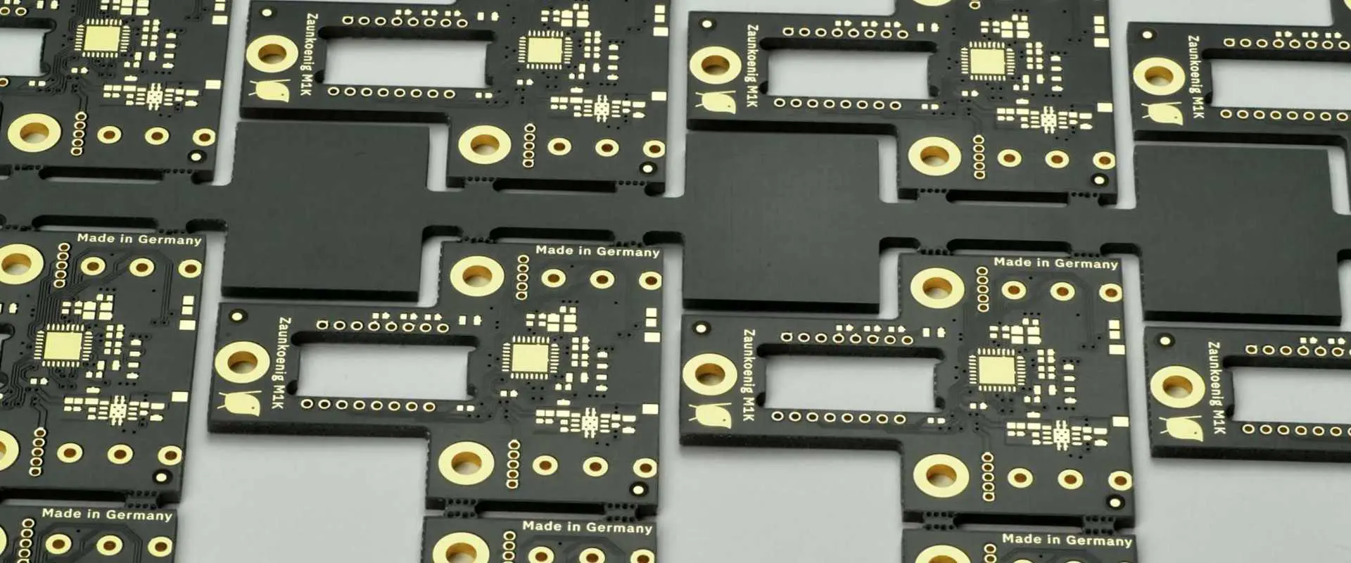
Description: A close-up image of a PCB panel showing breakaway tabs with perforations and a test coupon on the edge.
ALT Text: "PCB panel with breakaway tabs and test coupon for quality control"
Design for Manufacturability in Panelization
Design for manufacturability (DFM) is a critical aspect of panelization that ensures your designs are optimized for efficient production. By focusing on DFM principles, you can avoid common pitfalls and reduce manufacturing costs. Here are key considerations for design for manufacturability in panelization.
- Adhere to Manufacturer Specifications: Every manufacturer has specific panel size limits and tolerances. For example, some may require a minimum panel border of 10 mm, while others accept 5 mm. Always check these specs to avoid redesigns.
- Optimize for Automated Assembly: If your boards will undergo automated pick-and-place assembly, ensure fiducial marks are placed in consistent locations (e.g., 5 mm from panel corners) for accurate machine alignment. Also, keep component orientations consistent across boards in the panel.
- Reduce Depanelization Risks: For high-density designs with components near edges, use mouse bites (small perforated holes) on breakaway tabs to minimize stress during separation. A typical mouse bite design includes 5 holes of 0.5 mm diameter spaced 0.8 mm apart.
- Account for Thermal Expansion: During soldering processes like reflow, panels can experience thermal expansion. Design with materials that have a low coefficient of thermal expansion (CTE), such as FR-4 with a CTE of 14-17 ppm/°C, to prevent warping.
- Simplify Testing and Inspection: Group test points on each board in a consistent location within the panel to speed up automated optical inspection (AOI). This reduces setup time and improves inspection accuracy.
By prioritizing design for manufacturability in your panelization process, you can create designs that are not only functional but also cost-effective and easy to produce at scale.
Common Challenges in Multi-Board Panelization and How to Overcome Them
Even with careful planning, panelization can present challenges. Here are some common issues faced by PCB design engineers and practical solutions to address them.
- Board Misalignment During Assembly: Misalignment can occur if fiducials or tooling holes are incorrectly placed. Solution: Double-check fiducial placement (e.g., 1 mm diameter marks at least 5 mm from edges) and confirm tooling hole sizes (typically 3 mm) with your manufacturer.
- Damage During Depanelization: Components near edges may crack or break during separation. Solution: Increase edge clearance to 2-3 mm for sensitive components and use tab routing with mouse bites for gentler separation.
- Panel Warping: Uneven thermal expansion can warp panels, especially with large or thin designs. Solution: Use balanced stackups (e.g., symmetrical copper layers) and materials with consistent CTE values (around 15 ppm/°C for standard FR-4).
- Overcrowded Panels: Packing too many boards into a panel can lead to insufficient spacing for manufacturing tools. Solution: Maintain a minimum spacing of 2 mm between boards and adhere to border width requirements (5-10 mm).
By anticipating these challenges and applying the suggested solutions, you can avoid costly mistakes and ensure a smoother panelization process.
Tools and Software for PCB Panelization
Modern design software can simplify the panelization process by automating many of the steps involved. While specific brand names won’t be mentioned, most PCB design tools offer features like panel layout editors, fiducial placement, and DFM rule checks. Look for software that allows you to:
- Create custom panel layouts with drag-and-drop functionality.
- Generate breakaway tabs or V-Cut lines automatically.
- Export panelized designs in standard formats like Gerber or ODB++.
Using the right tools can save time and reduce errors, especially for complex multi-board designs. Additionally, many manufacturers provide free panelization utilities or templates to help engineers align their designs with production capabilities.
Conclusion: Elevate Your PCB Designs with Expert Panelization
Mastering multi-board panelization is an essential skill for PCB design engineers aiming to optimize production efficiency and reduce costs. By following this comprehensive guide, including our PCB panelization tutorial, multi-board design guidelines, panelization best practices, and tips for design for manufacturability, you can create panels that meet the highest standards of quality and performance.
Start by applying the basics of panelization to your next project, then refine your approach with advanced strategies like strategic board placement, DFM principles, and close collaboration with manufacturers. With practice, you’ll be able to tackle even the most complex multi-board designs with confidence, ensuring smooth production runs and exceptional results.
Panelization isn’t just a manufacturing step—it’s a design opportunity. Take the insights from this guide and transform your PCB projects into efficient, cost-effective solutions that stand out in the industry.


