ALLPCB


Are you looking to add a creative twist to your printed circuit board (PCB) designs? Inner layer PCB art, with hidden visuals embedded within the layers of a multi-layer board, offers a unique way to combine functionality with aesthetics. This blog dives deep into the world of PCB art, focusing on hidden PCB designs and creative PCB layouts. Whether you're an engineer, designer, or hobbyist, you'll find practical tips and inspiring ideas to elevate your next project with hidden visuals that surprise and delight.
What Is Inner Layer PCB Art?
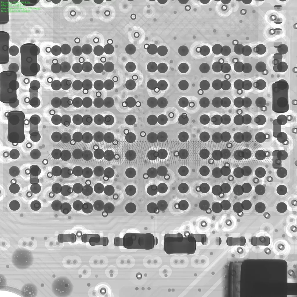
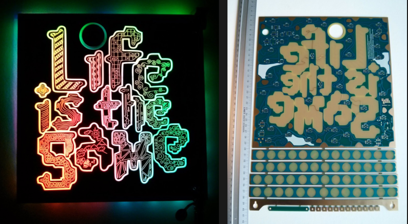
Inner layer PCB art refers to the practice of incorporating visual designs or patterns into the internal layers of a multi-layer PCB. Unlike surface-level artwork on the silkscreen or copper layers, these designs are hidden from plain sight, sandwiched between insulating substrates. They can only be seen under specific conditions, such as when the board is backlit, X-rayed, or disassembled.
This form of PCB art is a growing trend among designers who want to add a personal touch or branding element to their circuits without sacrificing functionality. Hidden PCB designs can include logos, intricate patterns, or even playful messages, making each board a work of art while maintaining its technical integrity. In this guide, we'll explore why inner layer art matters, how to create it, and the tools and techniques to bring your creative PCB layouts to life.
Why Choose Hidden PCB Designs?
Hidden PCB designs offer several benefits beyond just aesthetics. First, they allow designers to embed branding or unique identifiers without cluttering the visible surface of the board. This is especially useful for companies wanting to protect intellectual property or add a signature style that’s only visible to those in the know.
Second, inner layer art can serve as a debugging or alignment tool during manufacturing. For instance, specific patterns can help identify layer misalignments, ensuring precision in high-density designs. Finally, hidden visuals add an element of surprise and creativity, making your project stand out in a competitive field. Imagine a PCB that reveals a stunning geometric pattern when held up to the light—it's a small detail that leaves a lasting impression.
The Basics of Multi-Layer PCBs and Inner Layers
Before diving into designing hidden visuals, it's important to understand the structure of multi-layer PCBs. These boards consist of multiple layers of conductive copper and insulating material stacked together. A typical multi-layer PCB might have 4, 6, 8, or more layers, with the inner layers used for routing signals and power planes to reduce noise and improve performance.
For example, in a 6-layer PCB, layers 2 through 5 are inner layers, hidden between the top and bottom surfaces. These layers are ideal for embedding PCB art since they don't interfere with surface-mounted components or silkscreen markings. The copper traces on inner layers can be manipulated to form shapes or patterns without affecting the board's electrical performance, provided the design follows certain guidelines.
Key considerations include maintaining signal integrity and avoiding interference with critical traces. For high-speed designs, improper placement of art can affect impedance, which should ideally be controlled to values like 50 ohms for single-ended signals or 100 ohms for differential pairs. Always prioritize functionality over aesthetics to ensure the board operates as intended.
Challenges of Working with Inner Layers
Designing for inner layers comes with unique challenges. Unlike surface layers, inner layers can't be easily inspected or modified after manufacturing. Any errors in the artwork or trace placement might require a complete redesign, increasing costs and delays. Additionally, the manufacturing process for multi-layer boards involves precise lamination and alignment, so hidden PCB designs must account for potential shifts during production—often within tolerances of ±0.1 mm for high-quality fabrication.
Another challenge is ensuring the artwork doesn't disrupt critical signal paths. For instance, adding a large copper fill for a visual design might create parasitic capacitance, affecting signal timing. Designers must balance creativity with technical constraints to achieve both stunning visuals and reliable performance.
How to Design Hidden PCB Art for Inner Layers
Creating hidden PCB designs requires a mix of artistic vision and technical know-how. Below, we’ll walk through the steps to design creative PCB layouts with hidden visuals, ensuring they enhance rather than hinder your board’s functionality.
Step 1: Plan Your Design Concept
Start by brainstorming the type of artwork you want to include. It could be a company logo, a geometric pattern, or a subtle Easter egg for fellow engineers. Keep in mind that inner layer art is often revealed through specific viewing methods, like backlighting or X-ray imaging, so consider how the design will appear under those conditions.
For example, a simple grid pattern might look striking when backlit, while a detailed logo could be a hidden signature only visible during inspection. Sketch your idea on paper or use graphic design software to create a digital mockup before integrating it into your PCB layout.
Step 2: Choose the Right Layer for Your Art
Decide which inner layer will host your artwork. In a 4-layer PCB, for instance, layers 2 and 3 are inner layers. Select a layer that has minimal signal routing or power plane requirements to avoid interference. If your design includes multiple power planes, you might dedicate a small section of one plane to your artwork, ensuring it doesn’t disrupt voltage distribution.
Remember that copper thickness on inner layers is typically thinner than on outer layers—often around 0.5 oz/ft2 compared to 1 oz/ft2 on the surface. This affects how the artwork appears when viewed through specialized methods, so test different copper fills or trace widths (e.g., 0.2 mm for fine details) to achieve the desired effect.
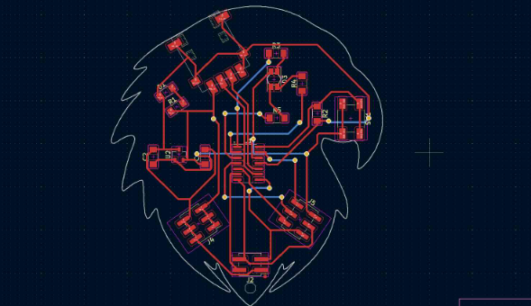
Step 3: Use PCB Design Software to Create the Art
Most PCB design tools allow you to manipulate copper pours, traces, and vias to create patterns. Start by importing your artwork as an image or vector file into the software. Then, convert the design into copper shapes or outlines on the chosen inner layer. Ensure the artwork adheres to the design rules for minimum trace width and spacing—often around 0.15 mm for standard manufacturing processes—to avoid fabrication issues.
For hidden visuals, consider using negative space. Instead of filling an area with copper, remove copper in specific shapes to create contrast when the board is backlit. This technique works well for logos or text, making them stand out against the surrounding copper plane.
Step 4: Validate Signal Integrity and Manufacturability
After placing your artwork, run a design rule check (DRC) to ensure it doesn’t violate manufacturing constraints or affect electrical performance. Pay attention to impedance control for high-speed signals, aiming for consistent values like 50 ohms on critical traces. If your artwork is near sensitive areas, simulate the board’s performance to detect potential issues like crosstalk or signal delay.
Additionally, consult with your fabrication partner to confirm that the hidden design won’t cause issues during lamination or drilling. Misalignment during layer stacking can distort the artwork, so ensure your design allows for small tolerances, typically within ±0.05 mm for advanced processes.
Creative Ideas for Hidden PCB Layouts
Looking for inspiration? Here are some creative PCB layouts and ideas for hidden visuals that can make your designs stand out.
- Branding Elements: Embed your company’s logo or a unique symbol on an inner layer as a subtle watermark. This adds a professional touch without cluttering the surface.
- Geometric Patterns: Use repeating shapes like hexagons or spirals to create mesmerizing effects when viewed under backlighting. These patterns can also double as alignment markers.
- Hidden Messages: Include a short phrase or code that’s only visible through X-ray or disassembly. This can be a fun way to engage with other engineers or hobbyists.
- Functional Art: Design copper pours that serve both aesthetic and practical purposes, such as improving heat dissipation while forming a visually appealing shape.
These ideas can be adapted to suit your project’s theme or purpose. The key is to experiment with different techniques while ensuring the artwork integrates seamlessly with the board’s functionality.
Tools and Techniques for Stunning Inner Layer Art
To achieve high-quality hidden PCB designs, you’ll need the right tools and techniques. Most professional PCB design software supports layer-specific editing, allowing you to create detailed artwork on inner layers. Look for features like image import, vector drawing, and copper pour manipulation to bring your vision to life.
Additionally, consider the viewing method for your hidden visuals. If the design is meant to be seen under backlighting, test different substrate materials—standard FR-4 with a thickness of 1.6 mm works well for light transmission. For X-ray visibility, ensure the copper density contrasts with the surrounding material, using heavier copper weights like 1 oz/ft2 for clearer images.
Finally, collaborate with your manufacturing partner to understand their capabilities. Some fabricators offer advanced imaging or laser etching for intricate inner layer designs, ensuring your artwork is reproduced with precision.
Best Practices for Balancing Art and Functionality
While hidden PCB art is exciting, it’s crucial to prioritize the board’s performance. Follow these best practices to ensure your creative PCB layouts don’t compromise functionality:
- Avoid Critical Areas: Keep artwork away from high-speed signal traces or power delivery zones to prevent interference. Maintain a clearance of at least 0.3 mm from sensitive areas.
- Minimize Copper Usage: Excessive copper in artwork can affect thermal balance or create unintended ground loops. Use sparse designs where possible.
- Test Iteratively: Prototype your design with a small batch to verify both the visual effect and electrical performance before full-scale production.
- Document Your Design: Clearly label the purpose of inner layer art in your design files to avoid confusion during manufacturing or assembly.
By adhering to these guidelines, you can create hidden PCB designs that are both visually stunning and technically sound.
Conclusion: Unleash Your Creativity with Inner Layer PCB Art
Inner layer PCB art offers a fascinating way to merge creativity with engineering. By embedding hidden visuals in your multi-layer boards, you can craft creative PCB layouts that surprise, inspire, and add value to your projects. From subtle branding to intricate patterns, the possibilities for hidden PCB designs are endless, provided you balance aesthetics with functionality.
Start small by experimenting with simple designs on a single inner layer, and gradually explore more complex ideas as you gain confidence. With the right tools, techniques, and manufacturing support, your hidden PCB art can transform a standard circuit board into a masterpiece. So, dive into the world of PCB art today, and let your inner layers tell a unique story.