ALLPCB


Designing a printed circuit board (PCB) requires precision, especially when it comes to minimum trace spacing. Using PCB design software like Altium or Eagle, you can ensure your traces meet the necessary spacing requirements to avoid electrical interference, signal issues, and manufacturing errors. This guide will walk you through the process of setting up and verifying minimum trace spacing using these powerful tools, with a focus on Design Rule Checks (DRC) to maintain design integrity.
In this comprehensive blog, we’ll dive deep into the importance of trace spacing, how to configure it in popular PCB design software, and tips for leveraging DRC to create reliable and efficient layouts. Whether you’re a beginner or an experienced engineer, you’ll find actionable steps to optimize your designs for performance and manufacturability.
What Is Minimum Trace Spacing and Why Does It Matter?
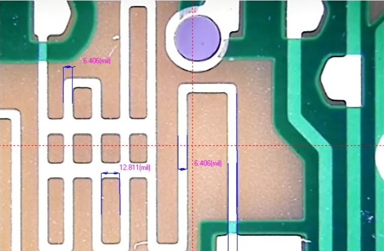
Minimum trace spacing refers to the smallest allowable distance between two conductive traces on a PCB. This spacing is critical to prevent issues like electrical shorts, crosstalk, and signal interference, especially in high-speed or high-voltage designs. The spacing requirements often depend on factors such as the voltage levels, signal frequencies, and manufacturing capabilities.
For example, in a low-voltage design operating at 5V, a trace spacing of 6 mils (0.006 inches) might be sufficient. However, for a high-voltage design handling 500V, you might need a spacing of 50 mils or more to prevent arcing. Failing to adhere to proper spacing can result in costly redesigns or board failures during testing or operation.
PCB design software plays a vital role in enforcing these spacing rules through automated checks and constraints. By setting up minimum trace spacing rules, you can ensure your design complies with industry standards and performs reliably under real-world conditions.
Understanding Design Rule Checks (DRC) in PCB Design Software
Design Rule Checks, or DRC, are automated tools in PCB design software that verify whether your layout adheres to predefined rules, including minimum trace spacing. DRC acts like a safety net, catching potential errors before you send your design for manufacturing. Without DRC, you might overlook small spacing violations that could lead to signal integrity problems or even complete board failure.
In software like Altium and Eagle, DRC settings allow you to define constraints for trace spacing, track width, via sizes, and more. Running a DRC after completing your layout helps identify and fix issues early, saving time and reducing costs.
Setting Up Minimum Trace Spacing in Altium Designer
Altium Designer is a leading PCB design software known for its robust rule-based design capabilities. Here’s a step-by-step guide to setting up and verifying minimum trace spacing in this tool.
Step 1: Access the PCB Rules and Constraints Editor
In Altium, the PCB Rules and Constraints Editor is where you define design rules. Open your PCB layout editor, then navigate to the "Rules" panel or access it via the menu under "Design > Rules." This editor allows you to create and customize rules for your specific project needs.
Step 2: Create a Clearance Rule for Trace Spacing
Within the Rules Editor, create a new rule under the "Electrical" category and select "Clearance." This rule governs the minimum spacing between traces, pads, and other conductive elements. Set the clearance value based on your design requirements. For instance, if you’re working on a 3.3V digital circuit, a clearance of 8 mils might be appropriate, while a power supply design may require 20 mils or more.
You can also apply this rule to specific net classes (e.g., high-voltage nets) to ensure different spacing requirements for different parts of your design. Use the query builder to filter nets by name or class for precise control.
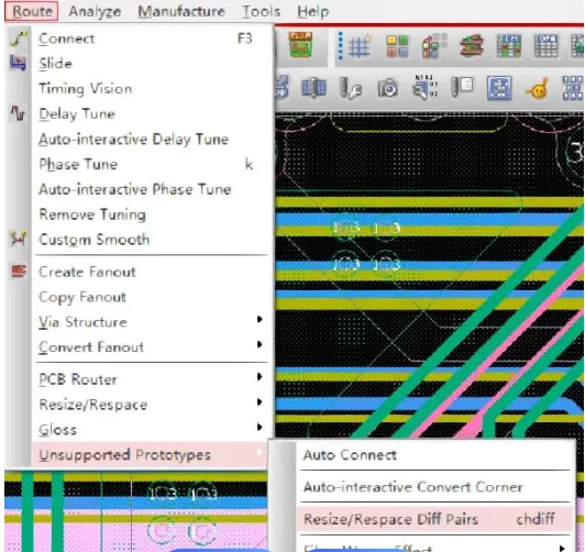
Step 3: Run a Design Rule Check
After setting the clearance rule, run a DRC to check for violations. Go to "Tools > Design Rule Check" and click "Run." The software will highlight any areas where traces are closer than the specified minimum spacing. Use the violation panel to zoom in on problem areas and adjust the layout as needed.
Configuring Minimum Trace Spacing in Eagle
Eagle is another popular PCB design software, especially among hobbyists and small teams, due to its user-friendly interface. Here’s how to manage trace spacing in Eagle.
Step 1: Open the Design Rules Window
In Eagle, design rules are managed through the "Design Rules" dialog. Open your board layout, then go to "Edit > Design Rules" or type "DRC" into the command line. This opens a window where you can configure various design parameters.
Step 2: Set Clearance Values
Navigate to the "Clearance" tab in the Design Rules window. Here, you can specify the minimum spacing between traces, pads, and vias. For a typical low-power design, a clearance of 6-8 mils is often sufficient. However, adjust this value based on your project’s voltage and signal requirements. Eagle allows you to set different clearances for different net classes if needed.
Step 3: Verify with DRC
Run a DRC by clicking the "Check" button in the Design Rules window or typing "DRC;" in the command line. Eagle will scan your layout and display any spacing violations in the errors list. Click on each error to locate the issue on the board and adjust the traces manually or use the autorouter with updated rules.
Factors Affecting Minimum Trace Spacing
When setting up trace spacing in PCB design software, consider the following factors to ensure your design meets both performance and manufacturing standards.
1. Voltage Levels
Higher voltages require larger trace spacing to prevent arcing or breakdown. For example, a design with 100V may need a minimum spacing of 30 mils, while a 5V design might only require 6 mils. Check industry standards like IPC-2221 for recommended clearance values based on voltage.
2. Signal Speed and Integrity
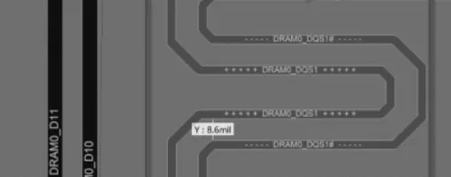
In high-speed designs, such as those with signals running at 1 GHz or higher, trace spacing affects crosstalk and impedance. Maintaining consistent spacing (often paired with controlled impedance routing) ensures signal integrity. For differential pairs, spacing might need to be as tight as 5 mils to match impedance requirements, while keeping enough distance from other traces to avoid interference.
3. Manufacturing Capabilities
Your manufacturer’s capabilities also dictate minimum trace spacing. Standard PCB fabrication processes often support spacing down to 6 mils, but advanced processes can handle 3 mils or less. Always consult your fabrication house for their specific limits before finalizing your design rules.
Tips for Optimizing Trace Spacing in PCB Layouts
Beyond setting rules in software, here are practical tips to ensure your trace spacing contributes to a high-quality PCB design.
1. Use Net Classes for Complex Designs
In both Altium and Eagle, you can assign different spacing rules to specific net classes. For instance, power nets might need larger spacing due to higher currents, while signal nets can have tighter spacing. This approach keeps your design organized and ensures compliance with varying requirements.
2. Leverage Autorouting with Caution
Autorouting tools can help place traces, but they might not always adhere to optimal spacing or routing patterns. After autorouting, run a DRC and manually inspect critical areas like high-speed signal paths or power traces to ensure proper spacing.
3. Test with Multiple DRC Runs
Don’t rely on a single DRC pass. Run checks at different stages of your design process—after initial placement, after routing, and before final export. This iterative approach catches issues early and ensures a clean layout.
Common Mistakes to Avoid with Trace Spacing
Even with powerful PCB design software, it’s easy to make mistakes if you’re not careful. Here are some common pitfalls and how to avoid them.
1. Ignoring Voltage-Dependent Spacing
One frequent error is applying the same spacing rule across all nets, regardless of voltage. This can lead to arcing in high-voltage areas. Always tailor spacing rules to the specific needs of each net or net class.
2. Overlooking Manufacturer Constraints
Designing with spacing below your manufacturer’s capabilities can result in production delays or defects. For instance, if your design uses 4-mil spacing but your fabricator only supports 6 mils, you’ll need to revise your layout. Double-check these limits early in the design phase.
3. Neglecting Signal Integrity for High-Speed Designs
In high-speed circuits, tight spacing can cause crosstalk, while excessive spacing can disrupt impedance matching. Use simulation tools or guidelines (like those for USB or HDMI signals) to balance spacing with performance.
How to Use DRC Reports for Continuous Improvement
DRC isn’t just a one-time check; it’s a tool for learning and refining your skills. After running a DRC, review the report in detail. Look for patterns in violations—are they mostly spacing issues, or do they involve other rules like track width? Use this feedback to adjust your design habits and improve future layouts.
In Altium, export the DRC report as a PDF or text file for documentation. In Eagle, save the error list for reference. Over time, you’ll develop an instinct for spacing and other design rules, reducing violations before they even occur.
Conclusion: Mastering Trace Spacing with PCB Design Software
Minimum trace spacing is a fundamental aspect of PCB design that directly impacts the reliability and performance of your board. By using PCB design software like Altium and Eagle, you can set up precise spacing rules, run DRC to catch errors, and optimize your layout for both functionality and manufacturability.
Start by understanding the specific needs of your project—voltage levels, signal speeds, and fabrication limits. Then, configure clearance rules in your software, verify with DRC, and iterate as needed. With these steps and tips, you’ll be well-equipped to create robust PCB designs that meet industry standards and perform flawlessly in the field.
At ALLPCB, we’re committed to supporting your design journey with resources and expertise. Use these guidelines to refine your trace spacing practices, and take your PCB designs to the next level.