 ALLPCB


In the world of electronics, where power demands are constantly rising, Heavy Copper PCBs have emerged as a go-to solution for high-power applications. If you're searching for insights on heavy copper PCB design guidelines, the heavy copper PCB manufacturing process, or the advantages of heavy copper PCBs, you're in the right place. This guide from ALLPCB offers a detailed look at how these specialized circuit boards can meet the needs of demanding projects, ensuring reliability and performance under extreme conditions.
Whether you're designing for industrial equipment, automotive systems, or renewable energy solutions, Heavy Copper PCBs provide the durability and current-carrying capacity required for success. In this comprehensive blog, we'll explore what makes these boards unique, how they're made, and why they're ideal for high-power environments. Let's dive in!
What Are Heavy Copper PCBs?
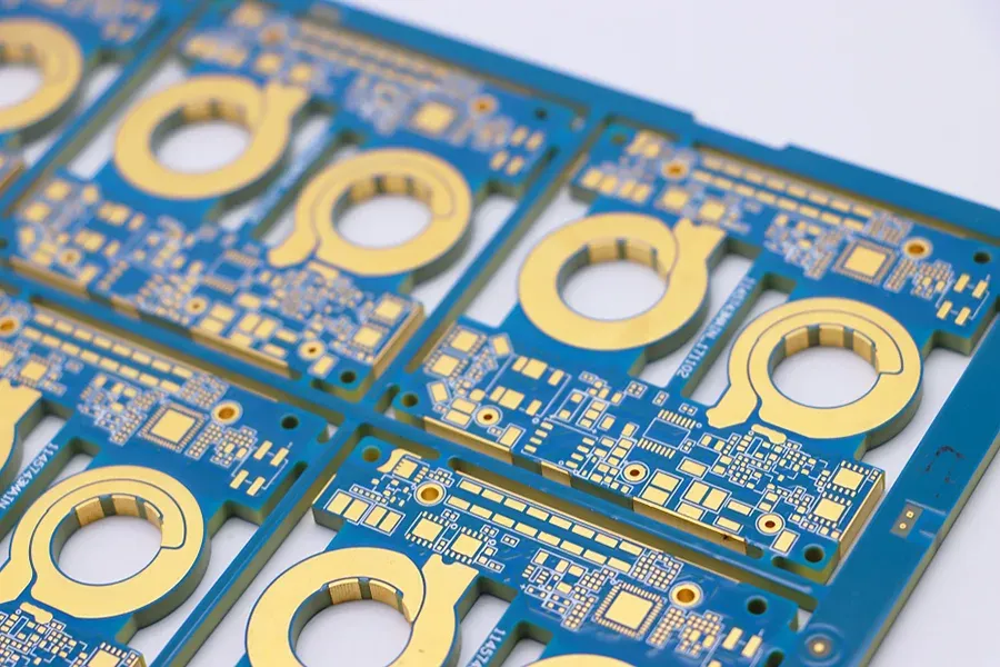
Heavy Copper PCBs are printed circuit boards that feature significantly thicker copper layers compared to standard PCBs. While a typical PCB might have copper layers ranging from 1 to 2 ounces per square foot (oz/ft2), Heavy Copper PCBs start at 3 oz/ft2 and can go up to 20 oz/ft2 or more. This increased copper thickness allows the board to handle higher current loads and dissipate heat more effectively, making them perfect for high-power applications.
These boards are often used in industries where reliability under stress is critical. Think of power supplies, electric vehicle (EV) systems, or solar inverters—environments where standard PCBs would fail due to overheating or electrical overload. By using thicker copper, these PCBs ensure that power is distributed efficiently without risking damage to the board or components.
Advantages of Heavy Copper PCBs for High-Power Applications
exploring the advantages of heavy copper PCBs in depth, it's clear why they are a preferred choice for high-power applications. Let's break down the key benefits that make them stand out.
1. Increased Current-Carrying Capacity
One of the primary advantages of Heavy Copper PCBs is their ability to carry higher currents without overheating. The thicker copper traces and planes can handle current loads that would cause standard PCBs to fail. For example, a 1 oz copper trace might safely carry around 1-2 amps per 10 mils of width, while a 6 oz copper trace can manage up to 6-12 amps for the same width, depending on thermal conditions. This makes them ideal for power electronics where high amperage is a constant requirement.
2. Superior Thermal Management
Heat dissipation is a major concern in high-power designs. Heavy Copper PCBs excel in this area by acting as a heat sink. The thicker copper layers spread heat more evenly across the board, reducing hot spots that could damage components or degrade performance. In applications like motor controllers, where heat generation can reach critical levels, these PCBs can withstand thermal cycling and maintain stability over time.
3. Enhanced Mechanical Strength
The added copper weight provides structural integrity to the PCB, making it more resistant to mechanical stress. This durability is crucial in environments subject to vibration or physical shock, such as automotive or industrial settings. A Heavy Copper PCB is less likely to crack or delaminate under such conditions, ensuring long-term reliability.
4. Improved Reliability for Repeated Thermal Cycles
In high-power applications, components often undergo repeated heating and cooling cycles during operation. Heavy Copper PCBs are designed to endure these thermal stresses without warping or losing conductivity. This reliability translates to fewer failures and lower maintenance costs over the product's lifecycle.
Heavy Copper PCB Design Guidelines
Designing a Heavy Copper PCB requires careful planning to maximize its benefits while avoiding common pitfalls. Below are essential heavy copper PCB design guidelines to follow for optimal performance in high-power applications.
1. Optimize Trace Width and Spacing
Given the high currents involved, trace widths must be calculated to handle the expected load without excessive heat buildup. A general rule of thumb is to increase trace width proportionally with copper thickness. For instance, a 3 oz copper layer might require traces at least 20-30% wider than a 1 oz layer for the same current. Additionally, spacing between traces should be increased to prevent arcing or short circuits, especially in high-voltage designs where dielectric breakdown is a risk.
2. Use Multiple Layers for Current Distribution
In multilayer designs, distribute high-current paths across several layers to balance the load and minimize resistance. For example, a 4-layer board with 4 oz copper on each layer can split a 20-amp current into roughly 5 amps per layer, reducing thermal stress on any single layer. Ensure vias are adequately sized and plated to handle the current between layers—undersized vias can become bottlenecks, leading to overheating.
3. Incorporate Thermal Vias and Heat Sinks
To enhance heat dissipation, integrate thermal vias near high-power components to transfer heat to copper planes or external heat sinks. A grid of vias, spaced at 0.3-0.5 mm intervals, can significantly lower the thermal resistance of the board. Pairing this with large copper pours on outer layers further aids in spreading heat evenly.
4. Account for Manufacturing Limitations
Heavy Copper PCBs have unique manufacturing constraints due to their thickness. Etching thicker copper requires more time and precision, which can limit the minimum trace width and spacing achievable. Typically, for a 6 oz copper layer, the minimum trace width might be around 0.015 inches (0.38 mm), compared to 0.006 inches (0.15 mm) for 1 oz copper. Consult with your fabrication partner early in the design phase to align your layout with their capabilities.
5. Balance Copper Distribution
Uneven copper distribution can lead to warping during manufacturing due to differential thermal expansion. Aim for symmetrical copper placement across layers and avoid large areas of solid copper on one side of the board without a corresponding feature on the opposite side. This balance helps maintain flatness and prevents assembly issues.
Heavy Copper PCB Manufacturing Process
Understanding the heavy copper PCB manufacturing process is crucial for engineers looking to integrate these boards into their projects. The process differs from standard PCB fabrication due to the challenges posed by thicker copper layers. Here's a step-by-step overview of how these boards are made.
1. Material Selection and Preparation
The process begins with selecting a suitable substrate, typically FR-4 or a high-Tg (glass transition temperature) material for better thermal stability. Copper foil, ranging from 3 oz/ft2 to 20 oz/ft2, is laminated onto the substrate. For extremely thick layers (above 6 oz), manufacturers may start with thinner foil and build up thickness through plating.
2. Imaging and Etching
A photoresist layer is applied to the copper surface, and the circuit pattern is transferred using UV light exposure through a photomask. The unexposed photoresist is washed away, leaving the desired trace pattern protected. Etching then removes the unprotected copper, a process that takes longer for heavier copper due to the increased material volume. Specialized etchants and longer processing times ensure clean, precise traces despite the thickness.
3. Plating for Added Thickness
For boards requiring copper beyond the initial foil thickness, electrolytic plating is used. The board is submerged in a copper sulfate solution, and an electric current deposits additional copper onto exposed areas. This step can build copper up to 10-20 oz/ft2 on outer layers, though it requires careful control to avoid uneven deposition or overplating.
4. Drilling and Via Formation
Holes for vias and component mounting are drilled using high-precision CNC machines. For Heavy Copper PCBs, via walls are plated with copper to ensure conductivity between layers, often requiring thicker plating (up to 2-3 mils) compared to standard boards (0.5-1 mil). This ensures the vias can handle high currents without failure.
5. Solder Mask and Surface Finish
A solder mask is applied to protect the copper from oxidation and prevent solder bridging during assembly. Due to the uneven surface created by thick copper, the mask application may require multiple coats for full coverage. Finally, a surface finish like HASL (Hot Air Solder Leveling) or ENIG (Electroless Nickel Immersion Gold) is added to enhance solderability and protect against corrosion.
6. Quality Inspection and Testing
Heavy Copper PCBs undergo rigorous testing to verify electrical continuity, insulation resistance, and thermal performance. Advanced techniques like microsectioning may be used to inspect via plating thickness and copper uniformity. Only boards meeting strict tolerances—such as ±10% variation in copper thickness—are approved for shipment.
Applications of Heavy Copper PCBs
Heavy Copper PCBs are indispensable in industries where high power and reliability are non-negotiable. Here are some common applications where their unique properties shine.
1. Power Electronics
In power supplies, converters, and inverters, these PCBs manage high currents and voltages while maintaining thermal stability. For example, a solar inverter handling 50 amps of continuous current relies on a Heavy Copper PCB to prevent overheating during peak operation.
2. Automotive and Electric Vehicles
Electric vehicles require robust battery management systems (BMS) and motor controllers capable of handling hundreds of amps. Heavy Copper PCBs ensure efficient power distribution and withstand the harsh conditions of automotive environments, including vibration and temperature swings from -40°C to 85°C.
3. Industrial Equipment
Heavy machinery and industrial automation systems often operate under high electrical loads. Heavy Copper PCBs in motor drives and control systems provide the durability needed for continuous operation in factories or mining operations.
4. Renewable Energy Systems
From wind turbines to energy storage systems, renewable energy applications demand PCBs that can handle fluctuating power levels. Heavy Copper PCBs support high-current connections and manage heat in compact, efficient designs.
Challenges and Considerations
While Heavy Copper PCBs offer significant advantages, they come with challenges that engineers must address during design and fabrication.
Cost: The increased material usage and specialized manufacturing processes make these PCBs more expensive than standard boards. A 6 oz copper board might cost 2-3 times more than a 1 oz board of the same size.
Weight: The added copper increases the board's weight, which can be a concern in weight-sensitive applications like aerospace. A 10 oz copper PCB can weigh nearly 10 times more per square foot than a 1 oz board.
Fabrication Complexity: Not all manufacturers have the equipment or expertise to handle extremely thick copper. Features like fine-pitch traces or dense via patterns may be limited, requiring design compromises.
Conclusion
Heavy Copper PCBs are a game-changer for high-power applications, offering unmatched current-carrying capacity, thermal management, and durability. By following heavy copper PCB design guidelines, engineers can create boards that meet the rigorous demands of industries like automotive, renewable energy, and industrial automation. Understanding the heavy copper PCB manufacturing process ensures that designs are aligned with fabrication capabilities, resulting in reliable, high-performance products. The advantages of heavy copper PCBs—from enhanced reliability to superior heat dissipation—make them an essential tool for tackling today's most challenging electronic designs.
At ALLPCB, we're committed to supporting your projects with top-quality fabrication services tailored to heavy copper requirements. Whether you're scaling up for production or prototyping a new high-power design, our expertise and advanced manufacturing capabilities are here to help you succeed.


