 ALLPCB


In the fast-evolving world of electronics, the demand for compact, lightweight, and adaptable solutions is at an all-time high. This is where flexible double-sided PCBs come into play. These innovative circuit boards offer a unique blend of flexibility and functionality, making them a top choice for modern designs. If you're wondering what a flexible double-sided PCB is, it's a type of printed circuit board with conductive traces on both sides, built on a flexible substrate that can bend and conform to various shapes without breaking. In this blog, we'll dive deep into the world of flexible PCB design, explore flex PCB applications, and uncover the intricacies of flex PCB manufacturing. Whether you're an engineer or a designer, this guide will provide valuable insights to help you leverage these versatile components in your projects.
What Are Flexible Double-Sided PCBs?
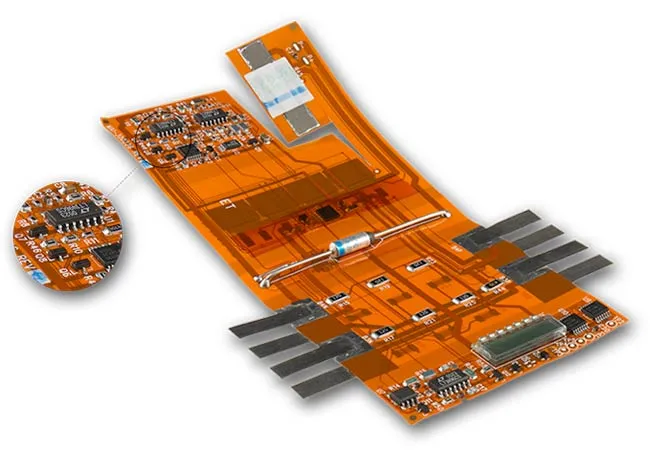
Flexible double-sided PCBs are a specialized category of printed circuit boards that feature conductive copper layers on both the top and bottom sides of a flexible base material, typically polyimide or polyester. Unlike rigid PCBs, these boards can bend, fold, and twist, allowing them to fit into tight or irregular spaces. The double-sided design doubles the surface area for components and traces compared to single-sided flex PCBs, enabling more complex circuits while maintaining a compact footprint.
The ability to place components on both sides also improves signal integrity and reduces the need for additional layers, which can save on costs and weight. These PCBs are often used in applications where space constraints and mechanical stress are significant factors. From wearable devices to aerospace systems, the adaptability of flexible double-sided PCBs makes them indispensable in cutting-edge technology.
Advantages of Flexible Double-Sided PCBs in Design
The benefits of using flexible double-sided PCBs in electronic design are numerous. Let's break down some of the key advantages that make them a preferred choice for engineers.
- Space Efficiency: With conductive layers on both sides, these PCBs allow for higher component density in a smaller area. This is crucial for devices like smartphones or medical implants where every millimeter counts.
- Lightweight Construction: The materials used in flex PCBs, such as polyimide, are much lighter than traditional rigid board materials like FR4. This can reduce the overall weight of a device by up to 60%, which is vital in applications like drones or portable gadgets.
- Durability Under Stress: Flexible PCBs can withstand repeated bending and flexing without cracking. Some designs can endure over 200,000 bend cycles, making them ideal for dynamic applications like foldable electronics.
- Improved Thermal Management: The thin materials used in flex PCBs dissipate heat more effectively than thicker rigid boards, helping to maintain optimal operating temperatures in compact designs.
- Reduced Wiring Needs: By integrating connections directly into the board, flex PCBs eliminate the need for bulky cables and connectors, simplifying assembly and reducing failure points.
These advantages highlight why flexible double-sided PCBs are often chosen over rigid alternatives in modern electronics. Their ability to adapt to unique shapes and withstand mechanical stress opens up new possibilities in design innovation.
Key Materials in Flexible PCB Design
The performance of a flexible double-sided PCB largely depends on the materials used in its construction. Understanding these materials is essential for optimizing design and manufacturing processes.
- Base Substrate: Polyimide is the most common material due to its excellent thermal stability (up to 400°C) and flexibility. Polyester is another option, though it's less durable under high temperatures.
- Conductive Layers: Copper foil is typically used for the conductive traces. Rolled annealed copper is preferred for dynamic applications because of its ductility, allowing it to bend without breaking. For high-density designs, electro-deposited copper is used for its smoother surface and better adhesion.
- Adhesives and Coverlays: Adhesives bond the copper to the substrate, though adhesive-less processes are gaining popularity to reduce thickness and enhance flexibility. Coverlays, made of polyimide with an adhesive layer, protect the traces from environmental damage.
- Stiffeners: In areas where components are mounted, stiffeners like FR4 or polyimide are added to provide rigidity and support during assembly.
Choosing the right combination of materials ensures that the PCB meets the specific mechanical and electrical requirements of the application. For instance, a wearable device may prioritize thinner, lighter materials, while an automotive application might need enhanced thermal resistance.
Flex PCB Applications Across Industries
The versatility of flexible double-sided PCBs makes them suitable for a wide range of industries. Here are some prominent flex PCB applications where their unique properties shine.
- Consumer Electronics: Devices like smartphones, smartwatches, and earbuds rely on flex PCBs to fit complex circuits into tiny, curved spaces. Their ability to fold allows for innovative designs, such as foldable phone screens.
- Medical Devices: In healthcare, flex PCBs are used in wearable monitors, hearing aids, and implantable devices. Their lightweight and biocompatible materials ensure comfort and reliability for patients.
- Automotive Systems: Modern vehicles use flex PCBs in dashboard displays, sensors, and control units. Their resistance to vibration and temperature fluctuations (ranging from -40°C to 150°C) makes them ideal for harsh environments.
- Aerospace and Defense: Satellites, drones, and military equipment benefit from the reduced weight and high reliability of flex PCBs. They can withstand extreme conditions while maintaining signal integrity at frequencies up to 5 GHz in some designs.
- Industrial Equipment: Robotics and automation systems use flex PCBs to connect moving parts without the risk of wire fatigue. Their durability under constant motion is a key asset.
These examples demonstrate how flexible double-sided PCBs are transforming industries by enabling smaller, more efficient, and durable electronic solutions. Their adaptability ensures they meet the diverse needs of modern technology.
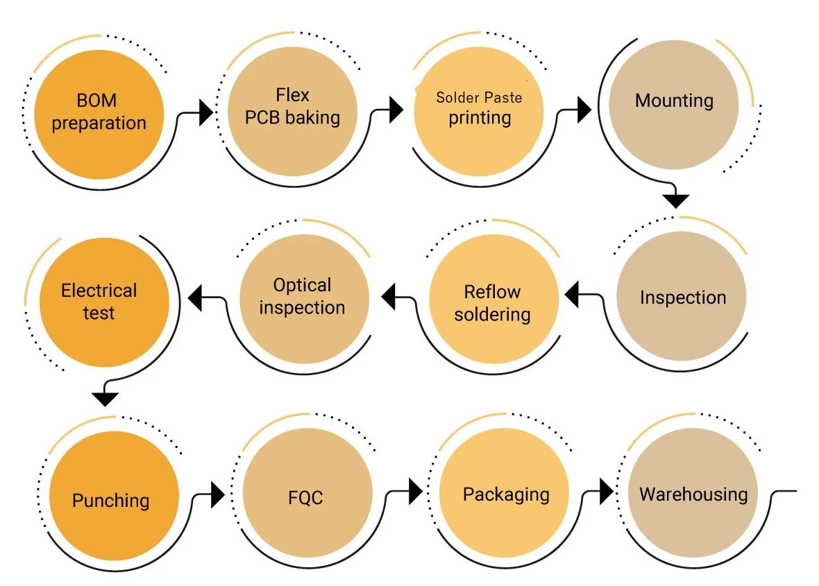
Flex PCB Manufacturing: A Step-by-Step Overview
The process of flex PCB manufacturing is intricate, requiring precision to ensure the board's flexibility and functionality. Here's a simplified look at the key steps involved in creating a flexible double-sided PCB.
- Design and Layout: The process begins with creating a detailed layout using specialized software. Designers must account for bend radii (typically a minimum of 6 times the board thickness) to prevent damage and ensure proper trace spacing (often 0.1 mm or more) to avoid shorts.
- Material Selection: As discussed earlier, choosing the right substrate, copper type, and protective layers is critical. Manufacturers often tailor materials based on the end application.
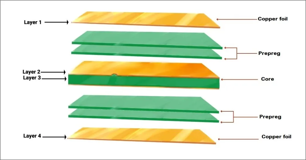
- Lamination: The copper foil is laminated onto the flexible substrate using heat and pressure. Adhesive-less lamination is increasingly used to reduce thickness, achieving total board thicknesses as low as 0.1 mm.
- Etching: Unwanted copper is removed through chemical etching to form the circuit pattern. This step requires precision to maintain trace widths, often down to 75 micrometers for high-density designs.
- Drilling and Plating: Vias are drilled to connect the top and bottom layers, then plated with copper to ensure conductivity. Via sizes can be as small as 0.2 mm in advanced processes.
- Coverlay Application: A protective coverlay is applied to shield the traces from moisture and debris, leaving openings for component pads.
- Testing and Inspection: The final board undergoes electrical testing and automated optical inspection (AOI) to detect defects. Impedance testing may also be conducted, targeting values like 50 ohms for high-speed signals.
Each step in flex PCB manufacturing requires careful attention to detail to ensure the board meets performance and durability standards. Collaboration with experienced manufacturers can help optimize the process for specific project needs.
Design Tips for Flexible Double-Sided PCBs
Creating an effective flexible PCB design requires careful planning to balance flexibility, functionality, and manufacturability. Here are some practical tips to guide your design process.
- Minimize Layer Count: While double-sided PCBs offer more space than single-sided ones, adding more layers increases thickness and reduces flexibility. Stick to two layers unless absolutely necessary.
- Optimize Bend Areas: Avoid placing components or vias in areas that will bend frequently. Maintain a bend radius of at least 6-10 times the board thickness to prevent cracking. For a 0.2 mm thick board, this means a minimum radius of 1.2-2 mm.
- Use Appropriate Trace Widths: Traces on flex PCBs are more vulnerable to damage. Maintain a minimum width of 0.1 mm and spacing of 0.1 mm to ensure reliability and prevent electrical shorts.
- Select Lightweight Components: Opt for surface-mount technology (SMT) components that are small and lightweight to avoid stressing the flexible substrate during bending.
- Incorporate Stiffeners: Add stiffeners in areas where connectors or heavy components are mounted to provide support and prevent tearing during assembly.
By following these guidelines, you can create a flexible double-sided PCB design that performs reliably while meeting the physical demands of your application.
Challenges in Flex PCB Design and Manufacturing
While flexible double-sided PCBs offer many benefits, they also come with unique challenges that engineers must address.
- Higher Costs: The specialized materials and manufacturing processes for flex PCBs can increase costs by 30-50% compared to rigid boards. Careful design optimization can help manage expenses.
- Mechanical Stress: Repeated bending can lead to fatigue in copper traces if not designed properly. Using rolled annealed copper and avoiding sharp bends can mitigate this risk.
- Complex Assembly: Assembling components on a flexible substrate requires precision to avoid misalignment. Automated pick-and-place machines are often necessary for accuracy.
- Signal Integrity Issues: High-speed signals, such as those above 1 GHz, may experience interference or loss due to the thin dielectric layers. Controlled impedance design and proper grounding are essential to maintain performance.
Understanding these challenges allows designers and manufacturers to take proactive steps to ensure the success of their flex PCB projects.
Future Trends in Flexible Double-Sided PCBs
The field of flexible PCB design and manufacturing is continuously evolving, driven by advancements in technology and growing demand for innovative electronics. Here are some trends to watch.
- Miniaturization: As devices become smaller, flex PCBs are being designed with even thinner materials and finer traces, pushing the limits of what's possible in compact electronics.
- Integration with Wearables: The rise of wearable technology is driving the development of flex PCBs with enhanced biocompatibility and stretchability for seamless integration into clothing and accessories.
- Sustainable Materials: Research is underway to develop eco-friendly substrates and manufacturing processes that reduce waste and eliminate harmful chemicals, aligning with global sustainability goals.
- Advanced Manufacturing Techniques: Innovations like laser-induced graphene and additive manufacturing are making it easier to produce flex PCBs with higher precision and lower costs.
These trends indicate a bright future for flexible double-sided PCBs, with endless possibilities for new applications and improved performance.
Conclusion
Flexible double-sided PCBs are revolutionizing the way we approach electronic design, offering unmatched adaptability and efficiency. From consumer gadgets to critical aerospace systems, their ability to fit into tight spaces, withstand mechanical stress, and support complex circuits makes them a game-changer in multiple industries. By understanding the materials, manufacturing processes, and design considerations, engineers can harness the full potential of flex PCBs to create innovative, reliable products.
Whether you're exploring flex PCB applications for a new project or refining your approach to flexible PCB design, the insights shared in this guide provide a solid foundation. With the right strategies and partnerships, you can navigate the challenges of flex PCB manufacturing and bring your ideas to life with precision and confidence. Embrace the flexibility of these remarkable boards and unlock new opportunities in your designs.


