 ALLPCB


In the world of modern electronics, the demand for smaller, faster, and more powerful devices continues to grow. Fine line PCB design and high-density interconnect (HDI) technology are at the heart of this evolution, enabling engineers to pack more functionality into compact spaces. If you're looking to understand fine line PCB design rules, HDI PCB design, or specifics like microvia design and trace width and spacing, you're in the right place. This guide will walk you through the essentials of designing high-density interconnect PCBs, offering practical tips and detailed insights to help you succeed.
At its core, fine line PCB design focuses on creating intricate circuit patterns with extremely narrow traces and tight spacing, often paired with HDI techniques like microvias to connect multiple layers efficiently. Whether you're working on a smartphone, wearable device, or advanced medical equipment, mastering these concepts is crucial. Let’s dive deeper into the principles, rules, and best practices that make high-density designs possible.
What Is Fine Line PCB Design and Why Does It Matter?
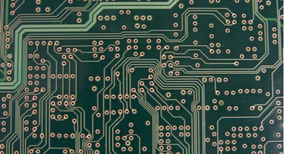
Fine line PCB design refers to the creation of printed circuit boards with very narrow trace widths and spacing, often below 100 micrometers (μm), to accommodate more components in a smaller area. This approach is a cornerstone of high-density interconnect PCB technology, which is widely used in compact electronics where space is at a premium.
The importance of fine line design lies in its ability to support the miniaturization of devices without sacrificing performance. For instance, in a typical smartphone, hundreds of components must fit into a tiny footprint while maintaining signal integrity and power efficiency. Fine line designs, combined with HDI techniques, make this possible by allowing more connections in less space.
Key Principles of HDI PCB Design
HDI PCB design goes beyond traditional PCB layouts by incorporating advanced features like microvias, blind vias, and buried vias to achieve higher wiring density. Here are the core principles to understand when working on such designs:
- Layer Stacking: HDI boards often use multiple layers with sequential lamination to create complex interconnections. For example, a design might feature a 2+N+2 structure, where "N" represents the core layers, and the numbers indicate additional build-up layers on each side.
- Microvias: These are small vias, typically less than 150 μm in diameter, drilled using laser technology. They connect adjacent layers, saving space compared to traditional through-hole vias.
- Fine Lines and Spacing: Achieving trace widths and spacing as small as 25 μm is now possible with advanced manufacturing, allowing for denser routing.
- Signal Integrity: High-density designs must minimize issues like crosstalk and electromagnetic interference (EMI) by carefully managing trace placement and impedance control.
By focusing on these elements, engineers can create boards that support high-speed signals, often exceeding 5 Gbps in applications like data communication devices, while maintaining reliability.
Fine Line PCB Design Rules for Success
Following fine line PCB design rules is essential to ensure manufacturability and performance. These rules address the challenges of working with narrow traces and tight tolerances. Below are some critical guidelines to keep in mind:
1. Trace Width and Spacing Standards
Trace width and spacing are the backbone of fine line designs. As traces get narrower, the risk of manufacturing defects or signal issues increases. Common standards include:
- Minimum trace width: Often as low as 50-75 μm for standard HDI designs, though advanced processes can achieve 25 μm.
- Minimum spacing: Matching or slightly larger than trace width, typically 50-100 μm, to prevent short circuits.
- Aspect ratio for vias: A ratio of 0.8:1 (via depth to diameter) is often recommended for microvias to ensure reliable plating.
For high-speed designs, maintaining consistent impedance (e.g., 50 ohms for single-ended signals or 100 ohms for differential pairs) is critical. Use simulation tools to calculate the required trace width based on the dielectric material and layer stack-up.
2. Material Selection
The choice of materials impacts both performance and manufacturability. High-frequency laminates with low dielectric constants (e.g., 3.5-4.0) and low loss tangents (e.g., 0.002-0.005) are ideal for maintaining signal integrity in HDI designs. Thin core materials, often less than 100 μm thick, also support finer lines and smaller vias.
3. Design for Manufacturability (DFM)
Work closely with your fabrication partner to align your design with their capabilities. For instance, confirm the minimum line width and spacing they can reliably produce. Many manufacturers struggle with traces below 50 μm without specialized equipment, so early collaboration can prevent costly redesigns.
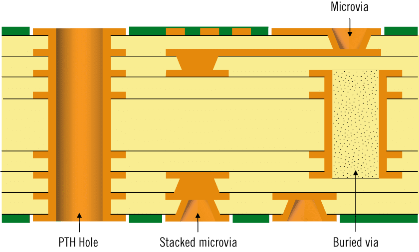
Microvia Design: A Critical Component of HDI
Microvia design plays a pivotal role in HDI PCBs by enabling connections between closely spaced layers without occupying much surface area. Unlike traditional vias that pass through the entire board, microvias are shallow, connecting only adjacent layers. Here’s what you need to know:
- Types of Microvias: Blind microvias connect an outer layer to an inner layer, while buried microvias connect internal layers only. Stacked microvias can link multiple layers for even denser designs.
- Size and Drilling: Microvias are typically 50-150 μm in diameter and are created using laser drilling for precision. This allows for smaller pads (e.g., 200-300 μm), freeing up space for routing.
- Reliability Concerns: Poorly designed microvias can suffer from issues like cracking or incomplete plating. Maintain a depth-to-diameter ratio below 1:1 to ensure structural integrity.
Proper microvia placement also helps reduce signal path length, which is crucial for high-speed applications. For example, in a 10-layer HDI board for a 5G module, microvias can cut signal delay by up to 20% compared to through-hole vias.
Challenges in Trace Width and Spacing for Fine Line Designs
Working with tight trace width and spacing introduces several challenges that engineers must address to avoid performance issues. Let’s explore these hurdles and how to overcome them:
1. Manufacturing Limitations
As trace widths shrink to 25-50 μm, fabrication becomes more complex. Etching processes must be precise to avoid over-etching, which can weaken traces or cause breaks. Always check with your manufacturer to confirm their minimum achievable dimensions—some may only support 75 μm traces reliably without additional costs.
2. Signal Integrity Risks
Narrow traces and close spacing increase the risk of crosstalk, where signals interfere with each other. To mitigate this, maintain a spacing-to-width ratio of at least 1:1 for low-speed signals and 3:1 for high-speed signals. Additionally, route critical signals on different layers or use ground planes to shield them.
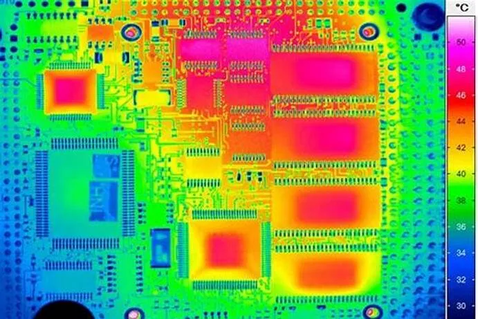
3. Thermal and Current Handling
Thinner traces have higher resistance, leading to greater heat generation. For a trace carrying 1 amp of current, a width of 50 μm on a 1 oz copper layer may overheat, risking delamination. Use trace width calculators to ensure your design can handle the expected current load without exceeding temperature limits (typically 10-20°C above ambient).
Best Practices for High-Density Interconnect PCB Layout
Creating a successful high-density interconnect PCB requires careful planning and execution. Here are some best practices to guide your layout process:
- Optimize Component Placement: Group related components together to minimize trace lengths. For example, place high-speed memory chips near the processor to reduce latency.
- Use Via-in-Pad Technology: Placing microvias directly under component pads saves space and improves routing efficiency, especially for fine-pitch components like BGAs with 0.4 mm spacing.
- Plan Power and Ground Planes: Dedicate entire layers to power and ground to provide stable voltage and reduce EMI. Split planes only when necessary for mixed-signal designs.
- Simulate Before Fabrication: Use software tools to simulate signal integrity, impedance, and thermal performance. Catching issues like reflections or hotspots early can save time and money.
Tools and Technologies for Fine Line and HDI Design
Designing fine line and HDI PCBs requires advanced tools to handle the complexity of tight tolerances and multilayer structures. Modern design software offers features like:
- Constraint-driven routing to enforce minimum trace width and spacing rules.
- 3D visualization to check layer alignment and via placement.
- Signal integrity analysis to predict and mitigate issues like crosstalk or delay.
Additionally, manufacturing technologies such as laser drilling for microvias and high-precision etching for fine lines have made it possible to push the boundaries of PCB density. Staying updated on these advancements can give your designs a competitive edge.
Conclusion: Mastering Fine Line PCB Design for HDI
Fine line PCB design and HDI PCB design are indispensable for creating the compact, high-performance electronics that define today’s market. By adhering to fine line PCB design rules, mastering microvia design, and carefully managing trace width and spacing, engineers can overcome the challenges of high-density interconnect PCBs and deliver reliable, efficient products.
Start by focusing on the fundamentals—optimize your trace dimensions, select the right materials, and collaborate with your manufacturer to align with their capabilities. With these strategies, you’ll be well-equipped to tackle even the most demanding HDI projects, ensuring your designs meet both performance and manufacturability goals.


