 ALLPCB


If you're looking to optimize a double-layer PCB stack-up while balancing performance and cost, you've come to the right place. In short, optimizing a double-layer PCB stack-up involves selecting the right materials, managing impedance for signal integrity, arranging layers for minimal interference, and keeping manufacturing costs in check. This blog dives deep into the details of achieving this balance, covering everything from material choices to impedance control and cost-effective design tips for your next project.
What Is a Double-Layer PCB Stack-Up?
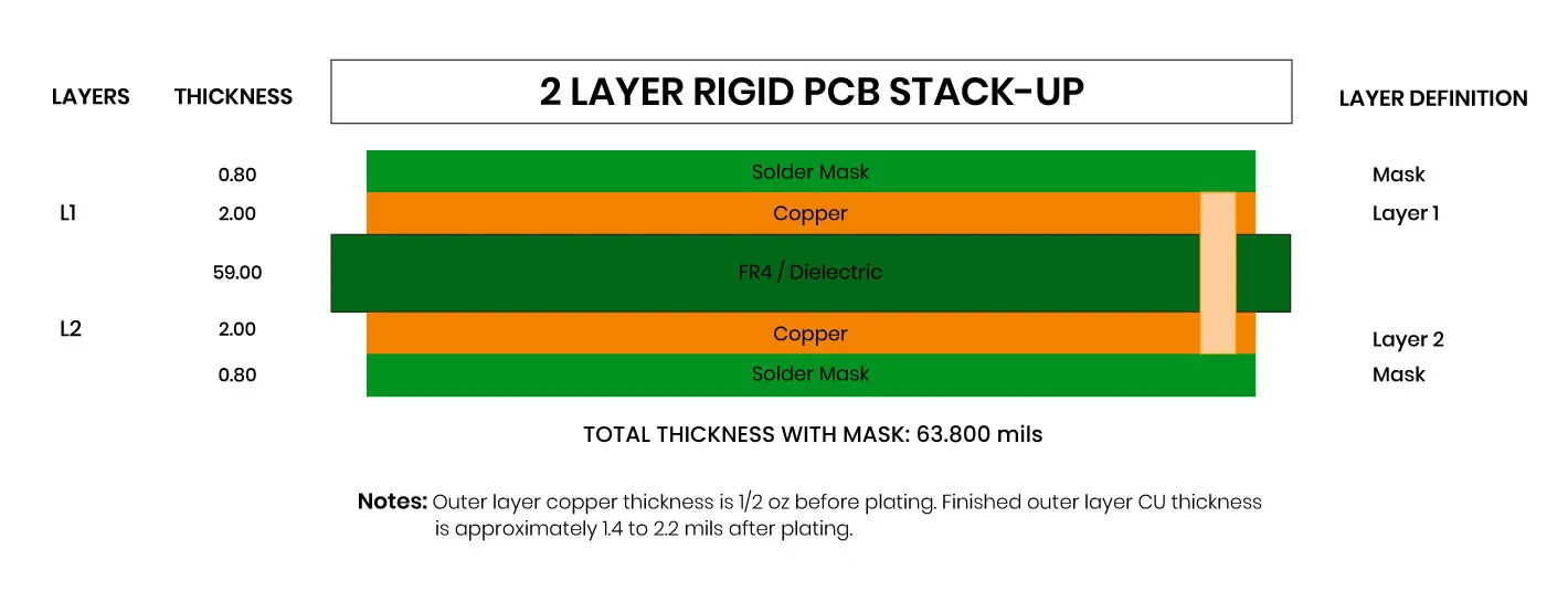
A double-layer PCB, often called a 2-layer PCB, is one of the simplest and most widely used printed circuit board designs. It consists of two conductive copper layers, typically separated by an insulating material known as the substrate or dielectric. These layers are used for routing signals, power, and ground connections, making them ideal for simpler electronic devices.
The stack-up refers to the arrangement of these layers and the materials used between them. Even though a double-layer PCB is less complex than multilayer designs, optimizing its stack-up is crucial for ensuring performance, signal integrity, and cost efficiency. A well-designed stack-up can reduce noise, prevent signal interference, and keep manufacturing expenses low, especially for high-volume production.
Why Optimize Double-Layer PCB Stack-Up?
Optimizing the stack-up of a double-layer PCB directly impacts both performance and cost. Without proper planning, you might face issues like signal distortion, electromagnetic interference (EMI), or higher production costs due to material choices or design inefficiencies. Here are the key reasons to focus on stack-up optimization:
- Signal Integrity: Proper layer arrangement and impedance control ensure signals travel without distortion, especially in high-speed applications.
- EMI Reduction: A good stack-up minimizes interference between signals and external noise sources.
- Cost Efficiency: Choosing the right materials and design strategies can significantly lower manufacturing expenses.
- Reliability: Optimized designs reduce the risk of failures, ensuring your product performs consistently over time.
Key Factors in Double-Layer PCB Stack-Up Optimization
Let’s break down the critical aspects of optimizing a double-layer PCB stack-up. These factors will help you achieve the best balance between performance and cost.
1. Material Selection for Double-Layer PCB Stack-Up
The choice of materials in a double-layer PCB plays a huge role in both performance and cost. The two primary materials to consider are the copper layers and the dielectric substrate between them.
- Copper Thickness: Common copper weights for double-layer PCBs are 1 oz (35 μm) or 2 oz (70 μm) per square foot. Thicker copper improves current-carrying capacity and heat dissipation but increases cost. For most applications, 1 oz copper is sufficient and cost-effective.
- Dielectric Material: The substrate material affects signal speed, impedance, and thermal performance. FR-4, a fiberglass epoxy laminate, is the most common choice for double-layer PCBs due to its low cost and decent electrical properties (dielectric constant around 4.2-4.5 at 1 MHz). For high-frequency applications, materials like Rogers or PTFE may be needed, but they come at a higher price.
When selecting double-layer PCB materials, consider the operating environment. For example, if your board will face high temperatures, ensure the material’s glass transition temperature (Tg) is adequate—FR-4 typically has a Tg of 130-140°C, which suits many applications.
2. Impedance Control in Double-Layer PCB Design
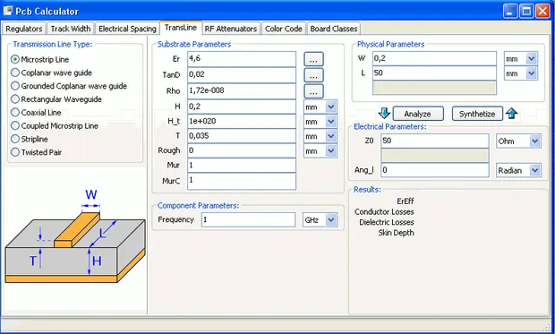
Impedance control is vital for maintaining signal integrity, especially in high-speed circuits. In a double-layer PCB, achieving controlled impedance can be challenging since there are only two layers to work with, and a dedicated ground plane isn’t always possible.
What is Impedance? Impedance, measured in ohms, is the resistance to the flow of alternating current in a circuit. For high-speed signals, traces on a PCB must have a specific impedance (often 50 ohms for RF applications or 100 ohms for differential pairs) to prevent signal reflections and loss.
In a double-layer PCB, impedance is influenced by:
- Trace Width and Thickness: Wider traces lower impedance, while thinner traces increase it. For a 50-ohm impedance on FR-4 with 1 oz copper, a trace width of about 0.011 inches (0.28 mm) is typical, assuming a dielectric thickness of 0.062 inches (1.6 mm).
- Dielectric Thickness: The distance between the trace and the reference plane (often the opposite layer) affects impedance. Thicker dielectric increases impedance.
- Dielectric Constant: Materials with a lower dielectric constant (like PTFE) allow for wider traces at the same impedance, which can be easier to manufacture.
To optimize double-layer PCB impedance, use simulation tools during the design phase to calculate trace dimensions. If a ground plane isn’t feasible on the second layer, dedicate areas of the bottom layer to ground and route signals on the top layer to maintain a consistent reference.
3. Layer Arrangement for Performance
In a double-layer PCB, you have limited options for layer arrangement compared to multilayer boards. However, how you assign signals, power, and ground to the layers still matters.
- Top Layer: Typically used for signal routing and component placement. Keep high-speed signals on this layer to minimize interference.
- Bottom Layer: Often used as a pseudo-ground plane or for power distribution. Flood unused areas with copper connected to ground to reduce EMI.
A common strategy is to route critical signals on the top layer and use the bottom layer for ground and power traces. This setup mimics a microstrip transmission line, helping with double-layer PCB impedance control. Avoid crossing high-speed signals on different layers without proper vias, as this can introduce noise.
4. Balancing Performance with PCB Layer Stack-Up Cost
Cost is a major concern when designing a double-layer PCB. While performance is important, over-engineering can lead to unnecessary expenses. Here are some tips to manage PCB layer stack-up cost:
- Stick to Standard Materials: FR-4 is widely available and cheaper than high-performance materials. Only opt for alternatives if your application demands it (e.g., high-frequency signals above 1 GHz).
- Minimize Copper Weight: Use 1 oz copper unless your design requires higher current capacity. Each additional ounce of copper can increase costs by 10-20%.
- Optimize Board Thickness: A standard thickness of 1.6 mm is cost-effective and widely supported by manufacturers. Thinner or thicker boards may require special processing, raising costs.
- Simplify Routing: Reduce the number of vias and complex trace patterns. Each via adds to drilling costs, and intricate designs may require tighter manufacturing tolerances.
For a typical double-layer PCB project, using FR-4 with 1 oz copper and a 1.6 mm thickness can keep costs around $0.50 to $1.00 per square inch for moderate volumes. Costs rise with specialized materials or tighter impedance tolerances (e.g., ±10% impedance control can add 15-25% to the price).
Suggested Image Placement: Place a cost comparison table or graph here showing material and thickness options versus price. ALT Text: "Cost comparison of double-layer PCB stack-up materials and configurations."
Design Tips for Double-Layer PCB Stack-Up Optimization
Here are actionable design tips to help you get the most out of your double-layer PCB stack-up while keeping costs low:
- Use Ground Pour: Fill unused areas on both layers with copper connected to ground. This reduces EMI and improves signal return paths, mimicking a ground plane.
- Route High-Speed Signals First: Prioritize critical signals during layout to avoid long detours or crossings that degrade performance.
- Keep Traces Short: Shorter traces reduce signal delay and loss. For high-speed designs, aim for trace lengths under 1/10th of the signal wavelength.
- Avoid Overlapping Power and Signal Traces: Separate power and signal traces to minimize crosstalk. If unavoidable, route them perpendicularly.
- Test Impedance Early: Use simulation software to verify impedance before fabrication. Correcting issues post-production is costly and time-consuming.
Common Challenges in Double-Layer PCB Stack-Up Design
Even with careful planning, designing a double-layer PCB stack-up comes with challenges. Being aware of these can help you avoid pitfalls:
- Limited Layer Count: Without dedicated ground or power planes, managing EMI and impedance is harder. Use ground pours and careful routing to compensate.
- Signal Crosstalk: With only two layers, signals can interfere if not spaced properly. Maintain at least 3 times the trace width as spacing between adjacent traces.
- Thermal Management: Double-layer PCBs have less copper for heat dissipation compared to multilayer boards. Use thicker copper or add thermal vias if heat is a concern.
Applications of Optimized Double-Layer PCBs
Double-layer PCBs are used in a wide range of applications due to their simplicity and cost-effectiveness. With proper stack-up optimization, they can deliver reliable performance in:
- Consumer Electronics: Devices like remote controls, simple sensors, and basic IoT gadgets often use double-layer PCBs for their low cost.
- Prototyping: Many engineers start with double-layer designs for initial prototypes before scaling to multilayer boards.
- Low-Speed Circuits: Applications with signal frequencies below 100 MHz can often work well on optimized double-layer PCBs without impedance issues.
Conclusion: Achieving the Perfect Balance
Optimizing a double-layer PCB stack-up is all about striking the right balance between performance and cost. By carefully selecting double-layer PCB materials, controlling double-layer PCB impedance, and following practical design tips, you can create a board that meets your project’s needs without breaking the budget. Focus on standard materials like FR-4, use ground pours for EMI reduction, and simulate impedance early to avoid costly redesigns.
Whether you're working on a simple prototype or a consumer product, a well-optimized stack-up ensures reliability and efficiency. Take the time to plan your design, and you’ll save both time and money in the long run. For more guidance on managing PCB layer stack-up cost or to start your next project with expert support, explore our resources and services tailored to your needs.


