 ALLPCB


Are you looking for a way to achieve a professional-grade PCB surface finish at home? If you're searching for "DIY ENIG," "homemade PCB finish," or an "alternative to ENIG PCB," you're in the right place. Electroless Nickel Immersion Gold (ENIG) is a popular surface finish for printed circuit boards (PCBs) due to its excellent solderability and corrosion resistance. However, replicating this process at home can be challenging due to the need for specialized chemicals and controlled environments. In this comprehensive guide, we'll explore practical alternatives to ENIG for home PCB fabrication, including "DIY gold plating" methods and other "PCB surface finish at home" techniques. Let's dive into the details of creating reliable, cost-effective finishes for your homemade PCBs.
What is ENIG and Why Look for Alternatives?
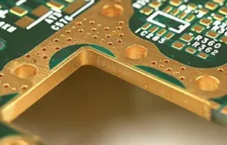
ENIG, or Electroless Nickel Immersion Gold, is a two-layer metallic coating applied to the copper surfaces of a PCB. It consists of a nickel layer that acts as a barrier to prevent copper diffusion, topped with a thin layer of gold to protect the nickel from oxidation. This finish is widely used in professional PCB manufacturing because it provides a flat surface for soldering, resists corrosion, and supports multiple reflow cycles without degrading.
However, DIY enthusiasts often find ENIG difficult to replicate at home. The process requires hazardous chemicals like nickel salts and gold cyanide solutions, precise temperature control, and proper waste disposal methods. Additionally, the cost of acquiring these materials can be prohibitive for hobbyists. This is why many home fabricators search for simpler, safer, and more affordable alternatives to achieve a durable and solderable PCB surface finish.
Challenges of DIY ENIG at Home
Before we explore alternatives, it’s important to understand the specific hurdles of attempting DIY ENIG. The process involves several complex steps, including:
- Cleaning: Removing all contaminants from the copper surface to ensure proper adhesion of the nickel layer.
- Electroless Nickel Plating: Depositing a uniform layer of nickel without an external electric current, which requires a carefully balanced chemical bath.
- Immersion Gold Plating: Applying a thin gold layer through a displacement reaction, where gold ions replace nickel on the surface.
Each step demands precision. For instance, the nickel bath typically operates at temperatures between 80-85°C (176-185°F), and even a slight deviation can result in uneven plating or poor adhesion. Moreover, the chemicals involved pose safety risks, requiring proper ventilation, protective gear, and disposal methods to avoid environmental harm.
Given these challenges, most home fabricators opt for alternative surface finishes that are easier to apply, use more accessible materials, and still provide acceptable performance for hobby projects.
Alternatives to ENIG for Homemade PCB Finish
Fortunately, there are several alternatives to ENIG that can be adapted for home use. Below, we’ll discuss some of the most practical options for achieving a reliable PCB surface finish at home. These methods focus on protecting the copper from oxidation and ensuring good solderability, even if they don’t fully replicate the durability of ENIG.
1. Hot Air Solder Leveling (HASL) at Home
Hot Air Solder Leveling, or HASL, is one of the most common PCB surface finishes in the industry and can be adapted for DIY use with some effort. In this method, the PCB is dipped into molten solder, and excess solder is blown off using hot air to create a thin, even layer. For home fabrication, you can mimic this process using a soldering iron and flux.
How to Apply HASL at Home:
- Ensure your PCB is clean and free of oxidation by lightly sanding the copper surface or using a chemical cleaner.
- Apply a thin layer of flux to the copper traces to improve solder adhesion and prevent oxidation during the process.
- Heat your soldering iron to around 260°C (500°F) and apply a thin layer of solder across the copper traces.
- Use the iron’s tip to spread the solder evenly, mimicking the leveling effect of hot air in professional setups.
- Remove excess solder with a desoldering braid if needed, aiming for a smooth, thin coating (ideally 1-5 micrometers thick).
Pros: HASL is inexpensive and uses readily available materials like solder and flux. It provides decent solderability for most hobby projects.
Cons: The finish may not be as flat as ENIG, which can cause issues with fine-pitch components. It also offers less corrosion resistance compared to gold-based finishes.
2. Tin Plating as a DIY Alternative
Tin plating, often referred to as immersion tin, is another viable alternative to ENIG for home PCB fabrication. This method involves coating the copper with a layer of tin to protect it from oxidation and improve solderability. Tin plating kits are sometimes available for hobbyists, or you can create a basic solution using tin chloride and other chemicals.
How to Apply Tin Plating at Home:
- Clean the PCB thoroughly to remove any dirt or oxide layers from the copper surface.
- Prepare a tin plating solution (follow safety guidelines if mixing your own) or use a pre-made kit. Typical solutions operate at room temperature or slightly warmed to 25-30°C (77-86°F).
- Immerse the PCB in the solution for 5-10 minutes, ensuring even coverage. Agitate the board gently to prevent uneven deposition.
- Rinse the PCB with distilled water and dry it carefully to avoid water spots.
Pros: Tin plating is relatively simple and provides a flat surface suitable for soldering. It’s also more accessible than gold plating for hobbyists.
Cons: Tin has a shorter shelf life compared to ENIG, as it can form whiskers (tiny metallic growths) over time, potentially causing short circuits. It’s best for projects that will be assembled soon after finishing.
3. DIY Gold Plating for PCB Surface Finish
For those determined to achieve a gold finish at home, DIY gold plating is possible, though it requires caution and careful handling of chemicals. This method won’t replicate the full ENIG process but can provide a thin gold layer over copper for improved corrosion resistance and aesthetics.
How to Apply Gold Plating at Home:
- Start with a clean PCB, free of any oxidation or contaminants on the copper surface.
- Acquire a gold plating solution or kit designed for small-scale use. These often include a gold salt solution and a mild electric current setup (electroplating rather than immersion).
- Set up a small electroplating station with a power supply (1-3 volts), an anode (often stainless steel), and your PCB as the cathode.
- Immerse the PCB in the solution and apply the current for 1-2 minutes, monitoring for even gold deposition (aim for a thickness of 0.05-0.1 micrometers).
- Rinse and dry the PCB carefully.
Pros: Gold plating offers excellent corrosion resistance and a professional appearance, closely mimicking one aspect of ENIG.
Cons: This method lacks the nickel underlayer of ENIG, so it’s less durable for repeated soldering. Safety is also a concern due to the chemicals involved.
4. Organic Solderability Preservative (OSP)
Organic Solderability Preservative, or OSP, is a water-based organic coating that protects copper from oxidation while maintaining solderability. It’s a simpler and safer option for home use compared to chemical plating methods.
How to Apply OSP at Home:
- Clean the PCB to remove any oxidation or contaminants from the copper traces.
- Apply an OSP solution (available in some hobbyist kits) by brushing or dipping the PCB. The process typically works at room temperature.
- Allow the coating to dry for the recommended time (usually 10-15 minutes), forming a thin protective layer (0.2-0.5 micrometers thick).
- Store the PCB in a dry environment until ready for soldering.
Pros: OSP is easy to apply, environmentally friendly, and provides a flat surface for soldering. It’s ideal for short-term storage of PCBs.
Cons: The coating is fragile and can degrade with handling or exposure to humidity, offering less long-term protection than ENIG or gold plating.
Comparing DIY PCB Surface Finish Options
To help you choose the best alternative to ENIG for your home PCB fabrication, here’s a quick comparison of the methods discussed:
| Finish Type | Ease of Application | Cost | Solderability | Corrosion Resistance | Durability |
|---|---|---|---|---|---|
| HASL (DIY) | Easy | Low | Good | Moderate | Moderate |
| Tin Plating | Moderate | Moderate | Good | Moderate | Low (whisker risk) |
| DIY Gold Plating | Difficult | High | Excellent | High | Moderate (no nickel layer) |
| OSP | Easy | Low | Good | Low | Low (fragile coating) |
This table highlights that no single method perfectly replicates ENIG, but each offers a balance of ease, cost, and performance suitable for different DIY projects. For instance, HASL and OSP are great for quick, budget-friendly projects, while tin or gold plating might suit applications needing better corrosion resistance.
Tips for Successful PCB Surface Finishing at Home
Regardless of the method you choose, here are some general tips to ensure a high-quality homemade PCB finish:
- Prioritize Safety: Always wear gloves, safety goggles, and work in a well-ventilated area when handling chemicals for plating or cleaning.
- Clean Thoroughly: A clean copper surface is critical for any finish. Use isopropyl alcohol or a mild abrasive to remove oxidation before starting.
- Test on Scrap Boards: Practice your chosen method on a small test piece before applying it to your final PCB to avoid costly mistakes.
- Control Environment: Work in a dust-free, low-humidity area to prevent contamination of the finish. For chemical processes, monitor temperature closely (e.g., 25-30°C for tin plating solutions).
- Store Properly: After finishing, store your PCBs in anti-static bags or containers to protect the surface until assembly.
When to Consider Professional Services
While DIY methods can work well for hobby projects, they often fall short of the reliability and consistency of professional ENIG finishes. If your project involves high-frequency signals (e.g., above 1 GHz), fine-pitch components (less than 0.5 mm spacing), or long-term reliability requirements, it might be worth investing in professional fabrication services. Professional ENIG finishes typically achieve nickel thicknesses of 3-6 micrometers and gold layers of 0.05-0.1 micrometers, ensuring optimal performance under demanding conditions.
For hobbyists on a budget, even professional services have become more accessible, offering affordable options for small batch production with high-quality finishes like ENIG. This can save time and reduce the risks associated with handling chemicals at home.
Conclusion: Finding the Right DIY PCB Finish for You
Achieving a professional-grade PCB surface finish at home doesn’t have to mean replicating ENIG exactly. By exploring alternatives like DIY HASL, tin plating, gold plating, or OSP, you can find a method that fits your skills, budget, and project needs. Whether you’re a beginner looking for a simple "homemade PCB finish" or an experienced maker experimenting with "DIY gold plating," the key is to prioritize safety, cleanliness, and patience during the process.
Each "alternative to ENIG PCB" discussed here offers unique benefits and trade-offs. HASL and OSP are ideal for quick, low-cost projects, while tin and gold plating provide better protection at the cost of complexity. With the right preparation and technique, you can create a reliable "PCB surface finish at home" that meets the demands of your DIY electronics projects. Start experimenting with these methods today, and elevate the quality of your homemade PCBs to the next level!


