ALLPCB


If you're designing a printed circuit board (PCB) and wondering how to determine the right trace width for optimal performance, you're in the right place. PCB trace width is crucial for maintaining signal integrity, managing impedance, and ensuring current capacity. In this comprehensive guide, we'll dive deep into PCB trace width calculation, signal integrity impedance, PCB trace current capacity, microstrip impedance, and stripline impedance. Whether you're a beginner or a seasoned engineer, this blog will provide actionable insights to help you design better PCBs.
Why PCB Trace Width Matters
PCB trace width is more than just a physical dimension on your board; it directly impacts how signals travel and how much current a trace can handle. A trace that's too narrow might overheat or fail to carry the required current, while a trace that's too wide could waste valuable board space or introduce unwanted impedance issues. Getting the width right ensures reliable performance, especially in high-speed designs where signal integrity impedance plays a critical role.
In the sections below, we'll break down the key factors influencing trace width and provide practical tips for calculating and optimizing it for your specific needs.
Understanding PCB Trace Width Calculation
Calculating the appropriate trace width for your PCB is a fundamental step in the design process. The width depends on several factors, including the current the trace needs to carry, the material of the board, and the operating environment. Let's explore how to approach PCB trace width calculation.
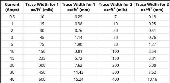
The primary concern when calculating trace width is ensuring it can handle the expected current without overheating. A widely used standard for this is based on industry guidelines, which correlate trace width to current capacity for a given temperature rise. For instance, a common rule suggests that for a 1 oz copper layer (1.4 mils thick), a trace width of 10 mils can handle approximately 1 ampere of current with a 10°C temperature rise. However, this can vary based on factors like ambient temperature and board thickness.
To calculate trace width more precisely, you can use online tools or formulas derived from standards like IPC-2221. These take into account:
- Current (in amperes): How much current the trace will carry.
- Copper thickness (in ounces per square foot): Thicker copper can handle more current.
- Temperature rise (in °C): The acceptable increase in temperature due to current flow.
- Trace length: Longer traces may require wider widths to manage heat dissipation.
For high-speed designs, trace width also affects impedance, which we'll cover later in this post. Balancing PCB trace current capacity with impedance requirements is key to a successful design.
Signal Integrity and Impedance: The Hidden Challenge
When it comes to high-speed circuits, signal integrity impedance becomes just as important as current capacity. Signal integrity refers to the quality of an electrical signal as it travels through a trace. Poor signal integrity can lead to issues like crosstalk, reflections, and data errors, especially in digital circuits operating at high frequencies.
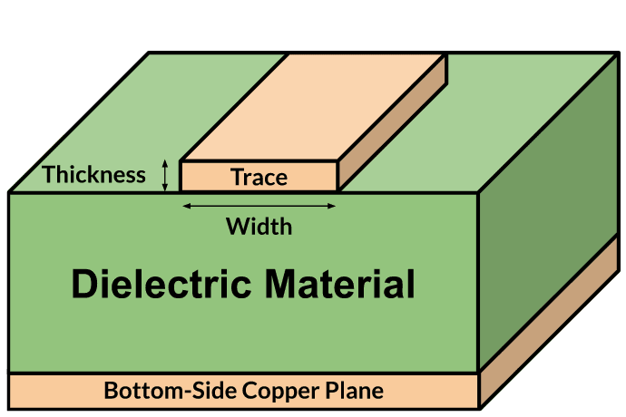
Impedance, measured in ohms, is a measure of opposition to the flow of alternating current in a circuit. In PCB design, controlling impedance ensures that signals are transmitted without distortion. Trace width, along with trace spacing, dielectric material, and layer stack-up, directly influences impedance. If the impedance isn't matched properly, signals can reflect back along the trace, causing interference.
For instance, in a high-speed USB design, a common target impedance for differential pairs is around 90 ohms. Adjusting the trace width and spacing is often necessary to achieve this value, depending on the board's dielectric constant (typically around 4.2 for standard FR-4 material) and layer thickness.
Maintaining signal integrity impedance requires careful planning during the design phase. Tools like impedance calculators can help determine the correct trace width and spacing for your specific application.
PCB Trace Current Capacity: How Much Can It Handle?
One of the most practical aspects of trace width design is ensuring it meets the PCB trace current capacity requirements. If a trace is too narrow for the current it carries, it can overheat, leading to potential damage or failure of the board.
As a general guideline, for a 1 oz copper layer, a trace width of 20 mils can handle about 2 amperes of current with a 10°C temperature rise. However, this capacity decreases with thinner copper or higher temperature rises. For a 2 oz copper layer, the same 20-mil trace can handle closer to 3.5 amperes under similar conditions.
Environmental factors also play a role. If your PCB operates in a high-temperature environment, you may need wider traces or additional cooling mechanisms to prevent overheating. Similarly, traces on inner layers of a multilayer board may have lower current capacity due to reduced heat dissipation compared to outer layers.
To ensure reliability, always design with a safety margin. For critical applications, consider increasing the trace width by 20-30% beyond the calculated minimum to account for manufacturing variations and unexpected current spikes.
Microstrip Impedance: Designing for Surface Traces
In PCB design, traces can be categorized into different types based on their position and configuration, each with unique impedance characteristics. One common type is the microstrip, which refers to traces on the outer layers of a PCB with a ground plane directly beneath them. Calculating microstrip impedance is essential for high-speed designs where signal integrity is critical.
Microstrip impedance depends on several factors, including trace width, trace thickness, the height of the dielectric material between the trace and ground plane, and the dielectric constant of the material. A typical formula for microstrip impedance (simplified for a narrow trace) is:
Z = (87 / √(Er + 1.41)) * ln(5.98 * H / (0.8 * W + T))
Where:
- Z is the impedance in ohms
- Er is the dielectric constant of the substrate (e.g., 4.2 for FR-4)
- H is the height of the dielectric (in mils)
- W is the trace width (in mils)
- T is the trace thickness (in mils)
For example, a microstrip trace with a width of 6 mils, a dielectric height of 10 mils, and a dielectric constant of 4.2 might have an impedance of approximately 50 ohms, a common target for many RF applications. Adjusting the trace width is often the easiest way to fine-tune impedance during design.
Microstrip traces are widely used due to their simplicity and accessibility on the board's surface, but they are more susceptible to external interference compared to other configurations. Proper impedance control is key to minimizing signal degradation.
Stripline Impedance: Buried Traces for Better Protection
Unlike microstrip traces, stripline traces are embedded between two ground planes within the PCB, offering better shielding from external noise. Calculating stripline impedance is crucial for designs where signal integrity and noise reduction are top priorities, such as in high-frequency or sensitive analog circuits.
Stripline impedance is influenced by trace width, trace thickness, the distance to both ground planes, and the dielectric constant. The formula for stripline impedance (simplified) is:
Z = (60 / √Er) * ln(1.9 * (2H + T) / (0.8 * W + T))
Where the variables are similar to those in the microstrip formula, but H represents the total dielectric height between the two ground planes. Stripline traces typically have lower impedance than microstrip traces for the same width due to the closer proximity of the ground planes.
For instance, a stripline trace with a width of 5 mils, a total dielectric height of 20 mils, and a dielectric constant of 4.2 might achieve an impedance of around 50 ohms. Stripline configurations are often used in multilayer boards where noise immunity is critical, though they can be more challenging to manufacture and test due to their buried nature.
Practical Tips for Optimizing Trace Width and Impedance
Designing a PCB with optimal trace width and impedance is a balancing act. Here are some practical tips to help you achieve the best results:
- Use Simulation Tools: Leverage design software with built-in impedance calculators to predict and adjust trace width for both microstrip and stripline configurations.
- Consider Manufacturing Tolerances: Trace widths can vary slightly during production. Design with a small margin to account for these variations, especially for impedance-critical traces.
- Plan Layer Stack-Up Early: The arrangement of layers and dielectric heights affects impedance. Define your stack-up before finalizing trace widths.
- Test Prototypes: For high-speed or high-current designs, build and test prototypes to verify that trace widths meet both PCB trace current capacity and signal integrity impedance requirements.
- Consult Standards: Refer to industry standards like IPC-2221 for current capacity and IPC-2141 for controlled impedance guidelines.
By following these tips, you can avoid common pitfalls and ensure your PCB performs reliably under real-world conditions.
Common Mistakes to Avoid in Trace Width Design
Even experienced designers can make mistakes when calculating trace width or impedance. Here are a few common errors to watch out for:
- Ignoring Temperature Rise: Failing to account for heat dissipation can lead to traces overheating, especially in power-heavy designs.
- Neglecting Impedance Matching: In high-speed designs, mismatched impedance can cause signal reflections and data loss.
- Overlooking Board Material: Different substrates have varying dielectric constants, which affect impedance. Always verify the material properties before calculating trace width.
- Using Arbitrary Widths: Guessing trace widths without calculations or tools can lead to performance issues. Always base your design on data.
Being mindful of these pitfalls can save you time and costly redesigns in the long run.
Conclusion: Mastering PCB Trace Width for Better Designs
Designing a PCB with the correct trace width is a critical step in ensuring both functionality and reliability. By understanding PCB trace width calculation, balancing PCB trace current capacity, and controlling signal integrity impedance, you can create boards that perform well in any application. Whether you're working with surface-level microstrip impedance or buried stripline impedance, the principles discussed in this guide provide a solid foundation for success.
Take the time to calculate, simulate, and test your designs. With careful planning and attention to detail, you can decode the complexities of PCB trace width and achieve optimal signal integrity in your projects.