 ALLPCB


Understanding minimum trace spacing is crucial for PCB designers aiming to ensure functionality, safety, and reliability in their designs. Whether you're concerned about high voltage safety, signal integrity, or adhering to industry standards, getting trace spacing right can make or break your project. In this guide, we'll break down the essentials of minimum trace spacing for high voltage, minimum trace spacing for signal integrity, minimum trace spacing IPC 2221 guidelines, and how to use a minimum trace spacing calculator to streamline your design process. Let's dive into the details to help you create robust and efficient PCB layouts.
What is Minimum Trace Spacing in PCB Design?
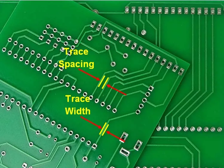
Minimum trace spacing refers to the smallest distance allowed between two conductive traces on a printed circuit board (PCB). This spacing is vital to prevent electrical issues like short circuits, arcing, or interference between signals. It directly impacts the safety and performance of a PCB, especially in applications involving high voltage or high-speed signals. Factors such as voltage levels, environmental conditions, and the type of signals being transmitted all influence the required spacing.
In the following sections, we'll explore how trace spacing applies to different design scenarios and provide practical insights for achieving optimal results. Whether you're a beginner or a seasoned designer, this guide will equip you with the knowledge to handle trace spacing challenges effectively.
Why Minimum Trace Spacing Matters in PCB Design
Trace spacing isn't just a random design rule—it's a fundamental aspect that ensures your PCB operates as intended. Improper spacing can lead to catastrophic failures, including electrical shorts, signal degradation, or even board damage due to arcing in high-voltage applications. By maintaining the correct spacing, you protect your design from these risks and ensure compliance with industry standards.
Beyond safety, trace spacing also affects manufacturing costs and board size. Tighter spacing can reduce the overall footprint of a PCB, but it often requires more precise fabrication techniques, which can increase costs. Balancing these factors is key to a successful design.
Minimum Trace Spacing for High Voltage Applications
When dealing with high voltage in PCB design, safety becomes the top priority. Minimum trace spacing for high voltage ensures that there's enough distance between conductive elements to prevent arcing or breakdown of the insulating material. The higher the voltage, the larger the spacing needs to be to avoid electrical discharge.
For instance, in designs operating at 500V, a spacing of at least 2.5mm might be necessary, depending on the dielectric strength of the PCB material and environmental factors like humidity or altitude. These values can increase significantly for voltages in the kilovolt range. High-voltage designs often require additional considerations, such as using wider traces or special coatings to enhance insulation.
One critical concept here is creepage and clearance. Creepage refers to the shortest path between two conductive parts along the surface of the insulating material, while clearance is the shortest distance through the air. Both must be accounted for in high-voltage designs to prevent unintended current flow. Industry standards provide specific guidelines for these distances based on voltage levels and application types, which we'll discuss in the context of IPC 2221 later.
Minimum Trace Spacing for Signal Integrity
In high-speed digital circuits or sensitive analog designs, minimum trace spacing for signal integrity plays a pivotal role in maintaining performance. When traces are too close, they can experience crosstalk, where signals from one trace interfere with another, leading to data errors or noise. Proper spacing helps minimize electromagnetic interference (EMI) and ensures clean signal transmission.
For example, in a design with high-speed signals operating at 1 GHz, a spacing of 3 times the trace width might be necessary to reduce crosstalk. This rule of thumb varies based on the signal frequency, dielectric constant of the board material, and trace geometry. Additionally, impedance matching becomes critical in such designs. Controlled impedance traces often require specific spacing to adjacent traces or ground planes to maintain a consistent characteristic impedance, such as 50 ohms for many RF applications.
To achieve optimal signal integrity, designers must also consider the layout of ground planes and the use of differential pairs, where traces carrying complementary signals are routed close together but with controlled spacing to external traces. These techniques help reduce noise and improve signal quality.
Understanding Minimum Trace Spacing with IPC 2221 Standards
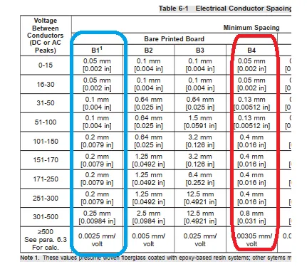
The minimum trace spacing IPC 2221 standard is a widely recognized guideline for PCB design, providing detailed requirements for trace spacing based on voltage, environmental conditions, and application type. IPC 2221, titled "Generic Standard on Printed Board Design," outlines safe spacing distances to ensure reliability and prevent electrical failures.
According to IPC 2221, trace spacing requirements are categorized based on whether the traces are on an external or internal layer and whether they are coated or uncoated. For example, for a voltage of 100V on an external layer without coating, a minimum clearance of 0.6mm is recommended. This value increases with higher voltages or harsher environmental conditions, such as high humidity or pollution levels, which can reduce the insulating properties of air or board materials.
The standard also provides tables and formulas to calculate creepage and clearance distances, factoring in the pollution degree and material group of the PCB. Designers working on high-voltage or safety-critical applications must adhere to these guidelines to ensure compliance and avoid costly redesigns or failures.
Using a Minimum Trace Spacing Calculator for Efficient Design
Manually calculating trace spacing for every scenario can be time-consuming and prone to errors, especially when dealing with complex designs. This is where a minimum trace spacing calculator becomes invaluable. These tools simplify the process by allowing designers to input parameters such as voltage, layer type, and environmental conditions to instantly get the recommended spacing values.
Many online calculators are based on industry standards like IPC 2221, ensuring that the results align with accepted guidelines. For instance, by entering a voltage of 300V and specifying an external uncoated layer, a calculator might output a minimum clearance of 1.5mm. Some advanced tools also account for signal integrity factors, providing spacing recommendations for high-speed designs to minimize crosstalk and EMI.
Using a calculator not only saves time but also reduces the risk of human error, ensuring that your design meets safety and performance requirements. These tools are especially useful during the early stages of layout planning, allowing you to quickly iterate and optimize your design.
Factors Influencing Minimum Trace Spacing
Several factors determine the appropriate trace spacing for a given PCB design. Understanding these can help you make informed decisions and create layouts that balance performance, safety, and manufacturability.
- Voltage Levels: Higher voltages require larger spacing to prevent arcing or dielectric breakdown. For example, a design operating at 1kV might need a clearance of 8mm or more, depending on the standard and conditions.
- Signal Frequency: High-frequency signals are more susceptible to crosstalk and EMI, necessitating wider spacing or specific routing strategies like differential pairs.
- Environmental Conditions: Factors like humidity, temperature, and pollution can affect the insulating properties of air and PCB materials, requiring larger spacing in harsh environments.
- Board Material: The dielectric strength and properties of the PCB substrate influence how much voltage it can withstand, impacting spacing requirements.
- Manufacturing Constraints: Tighter spacing can increase production costs due to the need for precision fabrication. Always check with your manufacturer for their capabilities and tolerances.
By considering these factors during the design phase, you can avoid common pitfalls and ensure your PCB performs reliably in its intended application.
Practical Tips for Implementing Minimum Trace Spacing
Now that we've covered the theory behind trace spacing, let's look at some actionable tips to apply these principles in your designs.
- Use Design Software with Built-in Rules: Modern PCB design softwares allow you to set spacing constraints based on voltage or signal type, automatically flagging violations during layout.
- Plan for Creepage and Clearance Early: Identify high-voltage areas in your schematic and allocate sufficient space during the initial layout to avoid cramped designs.
- Consult Industry Standards: Always refer to guidelines like IPC 2221 for spacing requirements, especially for safety-critical or high-voltage applications.
- Test and Validate: After completing your layout, perform design rule checks (DRC) and, if possible, prototype testing to verify that spacing meets performance and safety needs.
- Collaborate with Manufacturers: Work closely with your PCB fabricator to ensure your spacing design aligns with their manufacturing capabilities and tolerances.
Following these steps can help streamline your design process and reduce the likelihood of costly revisions or failures.
Common Mistakes to Avoid with Trace Spacing
Even experienced designers can make mistakes when it comes to trace spacing. Here are some common pitfalls to watch out for:
- Ignoring Environmental Factors: Failing to account for humidity or temperature variations can lead to insufficient spacing and potential failures in the field.
- Overlooking Internal Layers: Spacing rules differ for internal versus external layers. Internal layers often require less spacing due to better insulation, but this must still be calculated accurately.
- Neglecting Signal Integrity Needs: Focusing solely on voltage spacing while ignoring crosstalk or impedance issues can degrade performance in high-speed designs.
- Assuming Uniform Spacing: Not all traces on a PCB will have the same spacing requirements. High-voltage and high-speed traces may need unique considerations compared to low-power traces.
By staying vigilant and double-checking your design against standards and requirements, you can avoid these errors and create more reliable PCBs.
Conclusion: Mastering Minimum Trace Spacing for Better PCB Designs
Minimum trace spacing is a cornerstone of effective PCB design, influencing everything from safety in high-voltage applications to performance in high-speed circuits. By understanding the principles behind minimum trace spacing for high voltage, minimum trace spacing for signal integrity, and adhering to standards like minimum trace spacing IPC 2221, you can create designs that are both safe and efficient. Additionally, leveraging tools like a minimum trace spacing calculator can save time and enhance accuracy in your workflow.
Armed with the insights and tips provided in this guide, you're well-equipped to tackle trace spacing challenges in your next project. Prioritize safety, performance, and manufacturability, and you'll be on your way to designing PCBs that meet the highest standards of quality and reliability.


