ALLPCB


If you’re looking to design a printed circuit board (PCB) with specific dimensions, online tools make it easier than ever to create custom sizes, generate necessary files, and order prototypes quickly. Whether you’re a hobbyist or a professional engineer, using online PCB design software allows for custom PCB dimension input, generating Gerber files online, and ordering PCBs with custom sizes—all with quick turnaround PCB prototyping. In this guide, we’ll walk you through the entire process step by step, ensuring you can bring your unique designs to life with ease.
Why Choose Online Tools for Custom PCB Design?
Designing PCBs with custom sizes used to require expensive software and a steep learning curve. Today, web-based platforms have changed the game by offering accessible, user-friendly solutions. These tools let you input precise measurements, visualize your design in real time, and prepare manufacturing files without needing high-end hardware or software licenses. Plus, many integrate directly with manufacturing services for seamless ordering and fast prototyping.
Step 1: Selecting the Right Online PCB Design Software
The first step in creating a PCB with custom sizes is choosing a reliable online design platform. Look for tools that support custom PCB dimension input and offer features like layer management, component libraries, and file export options for manufacturing. Many web-based editors are free or low-cost, making them ideal for beginners and professionals alike.
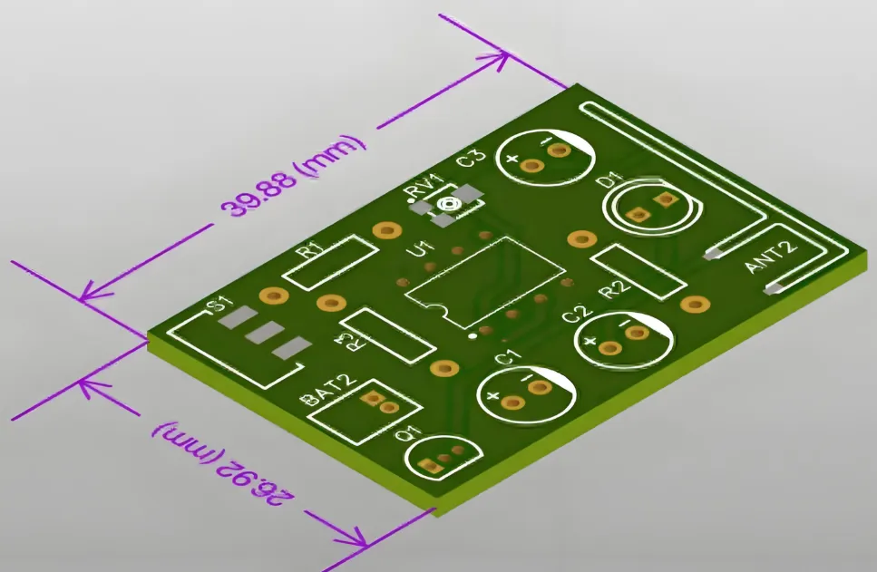
Ensure the platform allows you to define board outlines manually or through exact numerical inputs. This is critical for non-standard shapes or sizes, such as a 50mm x 75mm board for a compact IoT device or a circular PCB for a wearable gadget. A good tool will also provide real-time error checking to avoid issues like overlapping traces or components outside the defined area.
Step 2: Setting Up Custom PCB Dimensions
Once you’ve selected your online PCB design software, it’s time to input your custom dimensions. Most platforms have a dedicated section for defining the board outline. Here’s how to do it:
- Access the Board Outline Tool: Navigate to the layout editor and find the option to set the board shape. This is often under a “Board” or “Outline” tab.
- Input Exact Measurements: Enter your desired width and height, such as 100mm x 60mm, or draw the shape manually using a grid for precision.
- Define Non-Standard Shapes: For irregular designs, use the drawing tools to create curves or cutouts. For example, if designing a PCB for a handheld device, you might need rounded edges or specific mounting holes.
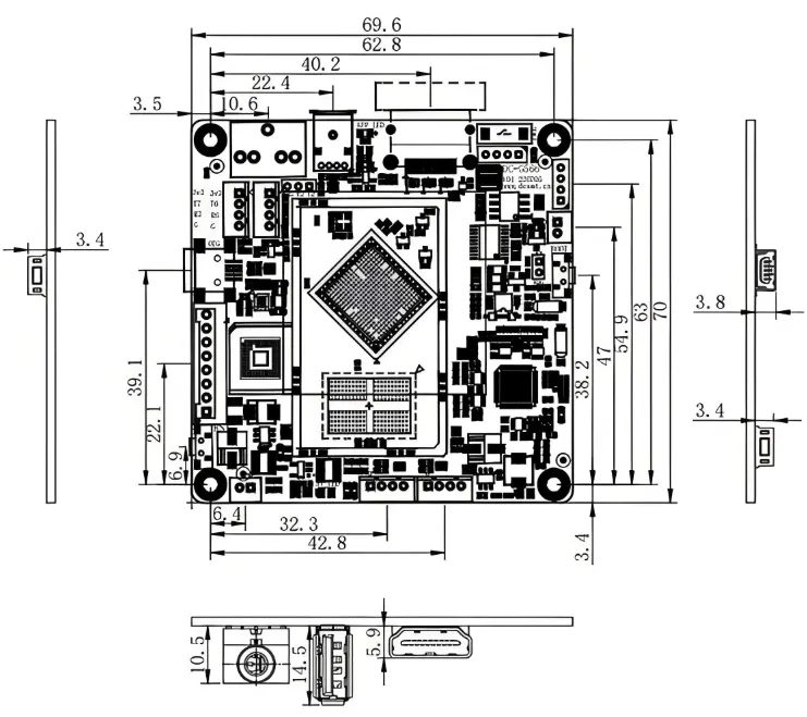
- Verify Constraints: Check that your dimensions meet manufacturing limits, such as minimum board thickness (often 0.6mm) or maximum size (sometimes up to 500mm x 500mm for standard services).
Accurate dimensions are crucial because they affect not only the fit of your PCB in its enclosure but also the signal integrity. For instance, a longer board might introduce delays in high-speed signals, requiring careful trace planning.
Step 3: Designing Your Circuit Layout
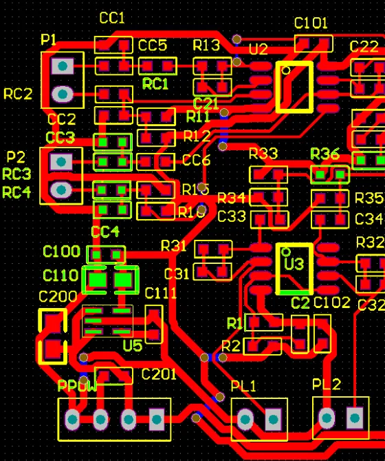
With your board size set, you can start placing components and routing traces. Online tools often come with extensive libraries of components, from resistors to microcontrollers, which you can drag and drop onto your board. Follow these tips for a successful layout:
- Place Critical Components First: Position high-priority parts like connectors or power regulators near their required locations to minimize trace length. For example, placing a USB connector at the edge of a 40mm x 80mm board reduces signal loss.
- Route Traces Efficiently: Keep high-speed signals (like those at 480 Mbps for USB 2.0) short and direct to avoid interference. Use impedance calculators if the tool offers them—aim for 50 ohms for most RF traces.
- Check Spacing Rules: Maintain proper clearance between traces (often 0.2mm or more) to prevent short circuits during manufacturing.
Take advantage of the software’s design rule check (DRC) feature to catch errors early. This ensures your custom-sized PCB will function as intended and meet fabrication standards.
Step 4: Generating Gerber Files Online
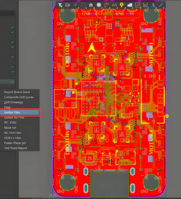
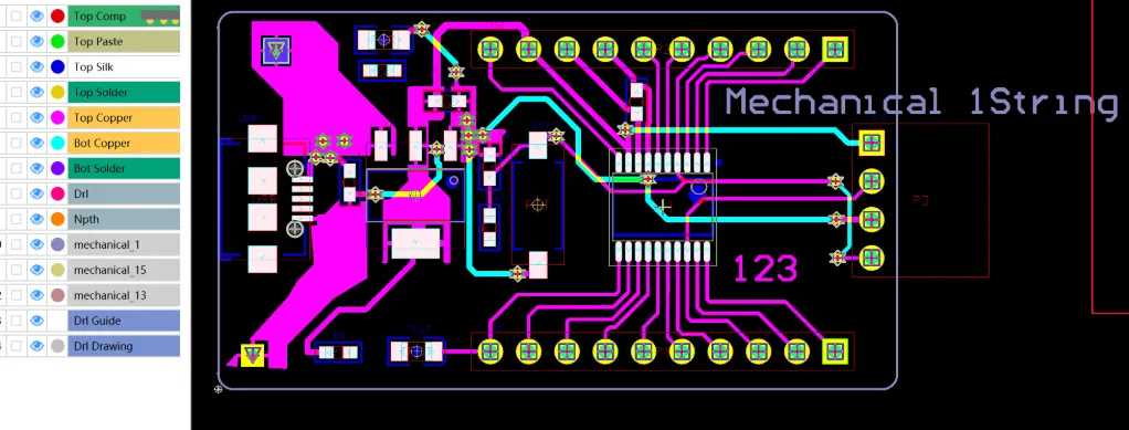
After finalizing your design, the next step is generating Gerber files online. Gerber files are the standard format used by manufacturers to produce your PCB. They include layers for copper traces, solder masks, silkscreen, and drill holes. Here’s how to create them using online tools:
- Access the Export Option: Look for a “Generate Manufacturing Files” or “Export” button in the design software.
- Select Layers: Choose all relevant layers for export, including top and bottom copper, drill data, and outline. Most tools automatically organize these into a zipped folder.
- Review Files: Many platforms offer a preview or viewer to ensure no layers are missing. Verify that your custom dimensions (e.g., a 65mm x 90mm board) are accurately reflected in the outline file.
- Download the Files: Save the zipped Gerber files to your device for uploading during the ordering process.
Some online platforms also generate additional files like the Bill of Materials (BOM) and pick-and-place data if you’re opting for assembly services. This streamlines the production process significantly.
Step 5: Ordering PCBs with Custom Sizes
With your Gerber files ready, you can move on to ordering PCBs with custom sizes. Many online design tools are integrated with manufacturing services, allowing you to upload files directly and get an instant quote. Follow these steps:
- Upload Gerber Files: Use the manufacturer’s online portal to upload your zipped Gerber folder. The system will analyze the files for errors and confirm your board dimensions.
- Specify Requirements: Choose options like board thickness (e.g., 1.6mm for standard designs), copper weight (1oz or 2oz), and surface finish (like HASL or ENIG for better durability).
- Select Quantity and Turnaround Time: For quick turnaround PCB prototyping, opt for expedited services, which can deliver in as little as 24-48 hours for small batches (e.g., 5-10 pieces).
- Review Cost and Place Order: Check the pricing—custom sizes may slightly increase costs due to material usage. Confirm everything before finalizing your order.
Double-check that the manufacturer supports your custom dimensions. Most standard services handle sizes from 10mm x 10mm up to large panels, but very small or oversized boards might require special handling.
Step 6: Verifying Your Design Before Production
Before production begins, take a moment to verify your design. Many manufacturers offer a free online viewer to inspect your uploaded Gerber files. Look for issues like misaligned drill holes or incorrect board outlines. For example, if your design is a 30mm x 50mm board with mounting holes at 2.5mm diameter, ensure they are positioned correctly to avoid assembly problems.
Additionally, run a final DRC if possible. This step can catch last-minute errors, such as a trace width below the minimum (e.g., 0.15mm when 0.2mm is required), saving you time and cost on revisions.
Tips for Quick Turnaround PCB Prototyping
When time is critical, quick turnaround PCB prototyping becomes a priority. Here are some strategies to speed up the process while maintaining quality:
- Opt for Standard Materials: Choosing common board materials like FR-4 and standard thicknesses (1.6mm) avoids delays in sourcing special materials.
- Minimize Complexity: Simplify your design by reducing layer count (e.g., sticking to 2 layers instead of 4) if possible, as multilayer boards take longer to produce.
- Plan Ahead for Components: Ensure your BOM is ready and components are in stock if you’re ordering assembly services. A missing 0.1μF capacitor can delay the entire project.
- Communicate with the Manufacturer: If you have tight deadlines, notify the service provider early. Many offer priority production for an additional fee.
Fast prototyping doesn’t mean sacrificing quality. By preparing accurate files and selecting efficient options, you can have your custom-sized PCB in hand within days.
Common Challenges with Custom PCB Sizes and How to Avoid Them
Designing and ordering PCBs with non-standard dimensions can come with hurdles. Here are a few common issues and solutions:
- Manufacturing Constraints: Some services have limits on minimum or maximum board sizes. Always check the specifications upfront. For instance, a board smaller than 5mm x 5mm might not be feasible without panelization.
- Cost Overruns: Custom sizes can increase material waste, raising costs. To save, consider designing multiple small boards on a single panel if the service allows it.
- Signal Integrity Issues: Larger or oddly shaped boards may affect high-frequency signals (e.g., above 100 MHz). Use ground planes and keep trace lengths under control to maintain impedance, targeting values like 50 ohms for RF designs.
By anticipating these challenges, you can ensure a smoother design-to-production journey for your custom PCB project.
Benefits of Using Online Tools for Custom PCB Design
Switching to online PCB design software offers several advantages, especially for custom projects:
- Accessibility: Work from any device with an internet connection—no need for powerful local hardware.
- Cost-Effectiveness: Many tools are free or subscription-based at a low cost, saving you from expensive standalone software.
- Integration: Direct links to manufacturing services mean you can design, generate files, and order all in one ecosystem.
- Community Support: Online platforms often have forums or tutorials to help troubleshoot issues like incorrect Gerber exports or layout errors.
These benefits make online tools a go-to choice for anyone looking to create PCBs tailored to specific dimensions.
Conclusion: Bring Your Custom PCB Vision to Life
Creating a PCB with custom sizes doesn’t have to be complicated. By leveraging online PCB design software, you can easily handle custom PCB dimension input, focus on generating Gerber files online, and succeed in ordering PCBs with custom sizes. With the added advantage of quick turnaround PCB prototyping, your ideas can move from concept to reality in record time.
Follow the steps outlined in this guide—selecting the right tool, setting dimensions, designing your layout, exporting files, and ordering with precision—to ensure a seamless process. Whether you’re crafting a tiny board for a wearable device or a large panel for industrial use, online tools empower you to achieve professional results without the traditional barriers. Start designing today and see how simple custom PCB creation can be!