 ALLPCB


If you're looking for ways to reduce costs in plated through-hole (PTH) manufacturing for printed circuit boards (PCBs), you're in the right place. This guide will share practical tips and tricks for reducing PTH cost, optimizing PTH drilling, minimizing PTH defects, PTH plating process optimization, and achieving overall PCB cost reduction. We'll dive into actionable strategies that can save time and money while maintaining high-quality results. Let’s explore how to streamline your PTH processes and improve efficiency without compromising performance.
Understanding Plated Through-Hole (PTH) Technology in PCB Manufacturing
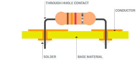
Plated through-hole technology is a cornerstone of PCB design, especially for multilayer boards. PTH involves drilling holes through the board and plating them with a conductive material, typically copper, to create electrical connections between layers. These holes also serve as mounting points for through-hole components. While PTH is essential for reliable connectivity, it can add significant costs to the manufacturing process if not managed carefully.
The main cost drivers in PTH manufacturing include drilling precision, plating materials, defect rates, and labor-intensive inspection processes. By focusing on cost-effective strategies, manufacturers can address these challenges and improve their bottom line. Let’s break down the key areas where savings and efficiency can be achieved.
Tip 1: Optimize PTH Drilling for Cost and Precision
Drilling is the first step in creating plated through-holes, and it’s a critical area for optimizing PTH drilling. Poor drilling practices can lead to misaligned holes, rough edges, or excessive wear on tools, all of which increase costs and defect rates. Here are some ways to improve drilling efficiency:
- Use High-Quality Drill Bits: Invest in durable, carbide-tipped drill bits designed for PCB materials like FR-4. These bits last longer and provide cleaner holes, reducing the need for rework. For example, a high-quality bit can drill up to 10,000 holes before needing replacement, compared to only 2,000 for cheaper alternatives.
- Control Drilling Speed and Feed Rate: Adjust the spindle speed and feed rate based on the board material and hole size. For standard FR-4 boards, a spindle speed of 80,000 RPM and a feed rate of 100 inches per minute can minimize burrs and heat buildup, extending tool life.
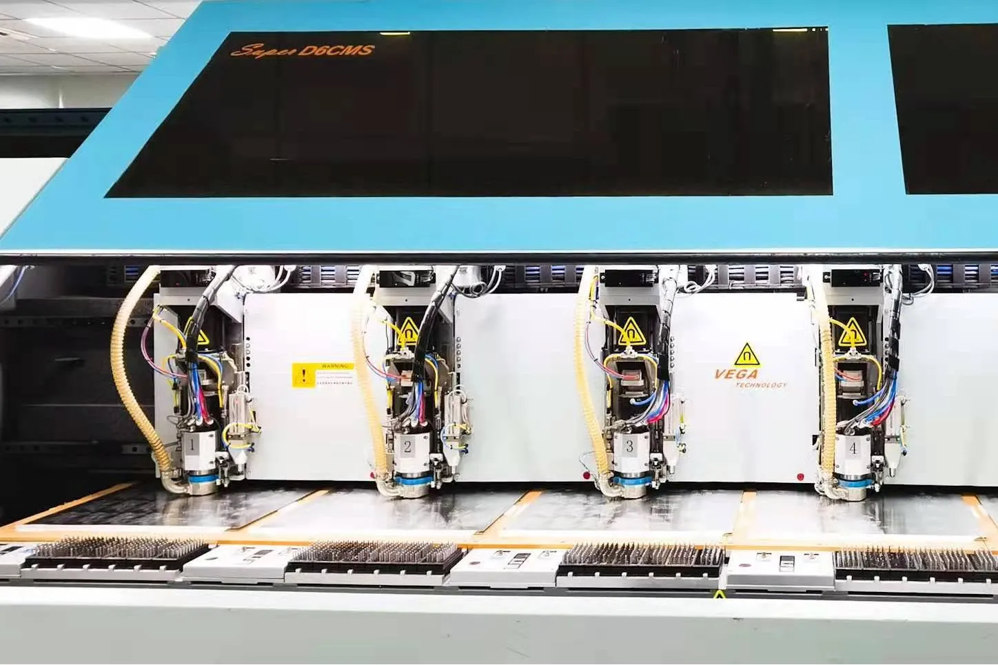
- Implement Automated Drilling Systems: Automated CNC drilling machines ensure precision and consistency, reducing human error. They also allow for faster production, lowering labor costs.
- Batch Similar Hole Sizes: Group holes of the same diameter in the design to minimize tool changes during drilling. This can cut setup time by up to 30%, directly impacting production costs.
By focusing on these drilling optimizations, you can achieve cleaner holes with less waste, paving the way for a smoother plating process and reducing PTH cost.
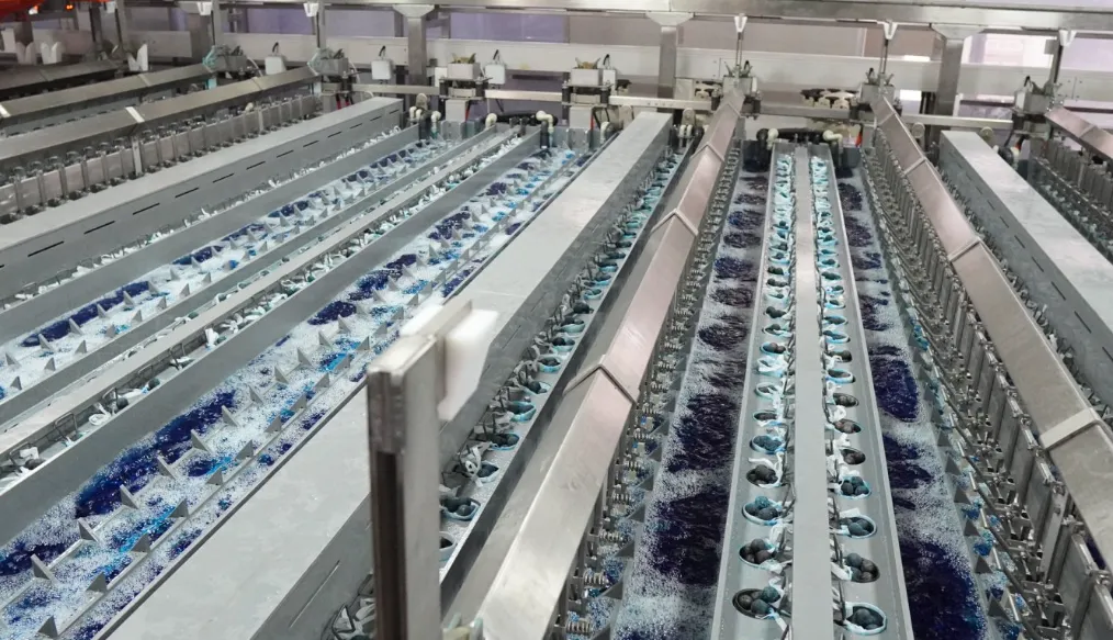
Tip 2: Streamline the PTH Plating Process for Efficiency
The plating process is where through-holes are coated with copper to ensure conductivity. However, inefficiencies in this stage can drive up costs due to material waste or uneven plating. PTH plating process optimization is key to maintaining quality while keeping expenses in check. Here’s how to do it:
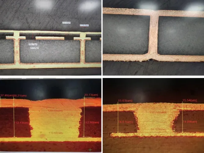
- Choose the Right Plating Thickness: Avoid over-plating by adhering to industry standards like IPC-6012, which recommends a copper thickness of 20-25 micrometers for most applications. Excess thickness increases material costs without adding significant value. For instance, increasing thickness from 25 to 30 micrometers can raise costs by 10-15% per board.
- Use Electroless Copper as a Base Layer: Start with a thin electroless copper layer (about 2-3 micrometers) to create a conductive surface before electrolytic plating. This method ensures uniform coverage in high-aspect-ratio holes (e.g., 8:1 ratio) and reduces the risk of voids.
- Monitor Bath Chemistry: Regularly test and adjust the chemical composition of plating baths to maintain consistent results. An unbalanced bath can lead to poor adhesion or uneven plating, requiring costly rework. Automated monitoring systems can help maintain pH levels between 12 and 13 for optimal performance.
- Reduce Plating Time: Optimize current density during electrolytic plating to speed up the process without sacrificing quality. A current density of 15-20 ASF (amperes per square foot) often strikes a good balance for standard PCBs, reducing plating time by up to 20%.
These steps ensure a reliable plating process that minimizes waste and rework, directly contributing to PCB cost reduction.
Tip 3: Minimize PTH Defects to Avoid Rework Costs
Defects in plated through-holes, such as voids, cracks, or insufficient plating, can lead to electrical failures and costly rework. Minimizing PTH defects is essential for maintaining quality and keeping production costs low. Here are practical ways to reduce defects:
- Deburr After Drilling: Remove burrs and debris from drilled holes using a deburring process or chemical cleaning. Rough edges can trap air or contaminants, leading to plating voids. A clean hole wall improves copper adhesion by up to 40%.
- Inspect Hole Quality Early: Use automated optical inspection (AOI) systems after drilling to detect misalignments or damage before plating. Catching issues early can save up to 50% of potential rework costs.
- Control Aspect Ratio: Design holes with a moderate aspect ratio (board thickness to hole diameter), ideally below 10:1. High aspect ratios make uniform plating difficult, increasing the likelihood of defects. For a 1.6mm thick board, aim for hole diameters no smaller than 0.2mm.
- Ensure Proper Cleaning: Before plating, clean holes with a plasma or chemical desmear process to remove resin smear caused by drilling. Smear can prevent proper copper deposition, leading to weak connections.
By focusing on defect prevention, you can avoid expensive rework and ensure reliable performance, supporting both quality and reducing PTH cost.
Tip 4: Design for Manufacturability to Lower Costs
Cost savings in PTH manufacturing often start at the design stage. By designing PCBs with manufacturability in mind, you can simplify production and reduce expenses. Here are some design tips for PCB cost reduction:
- Minimize Hole Count: Reduce the number of through-holes where possible by using surface-mount technology (SMT) for components. Fewer holes mean less drilling and plating, cutting costs by as much as 20% on complex boards.
- Standardize Hole Sizes: Stick to standard drill sizes (e.g., 0.3mm, 0.5mm, 1.0mm) to avoid custom tooling costs. Non-standard sizes can increase setup fees by 15-25% per order.
- Space Holes Appropriately: Maintain adequate spacing between holes (at least 0.5mm edge-to-edge) to prevent structural weakness or drilling errors. Tight spacing can lead to board breakage, increasing scrap rates.
- Avoid Unnecessary Layers: Limit the number of layers in multilayer boards unless absolutely necessary. Each additional layer adds to drilling and plating complexity, raising costs by 10-15% per layer.
Thoughtful design choices make manufacturing smoother and more cost-effective, directly impacting the overall budget for PTH processes.
Tip 5: Leverage Automation and Technology for Savings
Automation and modern technology play a big role in achieving reducing PTH cost. By integrating advanced tools and systems, manufacturers can boost efficiency and reduce manual labor. Here’s how technology can help:
- Automated Inspection Systems: Use AOI and X-ray inspection to detect defects in PTHs without manual checks. These systems can process up to 100 boards per hour, compared to 10-15 for manual inspection, saving significant labor costs.
- Software for Process Simulation: Use simulation tools to predict plating uniformity and identify potential issues before production. This can reduce trial-and-error costs by up to 30%.
- Robotic Handling: Implement robotic systems for loading and unloading boards during drilling and plating. This minimizes human error and speeds up production by 25-40%.
Investing in technology might have upfront costs, but the long-term savings and quality improvements make it a smart choice for cost-effective PTH manufacturing.
Tip 6: Partner with a Reliable Manufacturing Service
Choosing the right manufacturing partner can make a big difference in achieving PCB cost reduction. A trusted service provider will offer expertise, advanced equipment, and cost-saving solutions tailored to your needs. Look for a partner that provides:
- Transparent pricing with no hidden fees.
- Support for design optimization to minimize manufacturing challenges.
- High-quality materials and processes to reduce defects and rework.
- Fast turnaround times to keep your project on schedule.
Working with an experienced team ensures that every step of the PTH process, from drilling to plating, is handled efficiently and cost-effectively.
Conclusion: Achieving Cost-Effective PTH Manufacturing
Plated through-hole manufacturing doesn’t have to break the bank. By focusing on strategies like optimizing PTH drilling, PTH plating process optimization, minimizing PTH defects, and smart design practices, you can achieve significant PCB cost reduction. Start with small changes, such as standardizing hole sizes or improving drilling precision, and scale up to automation and technology for even greater savings.


