 ALLPCB


In the fast-paced world of electronics, high-speed printed circuit boards (PCBs) are the backbone of modern devices, from smartphones to data centers. A key challenge in designing these boards is maintaining signal integrity at high frequencies. One proven solution is controlled depth drilling, often referred to as back drilling, which minimizes via stubs to boost performance. This technique is vital for high-speed PCB back drilling, offering significant controlled depth drilling benefits by reducing signal distortion and electromagnetic interference (EMI). In this blog, we’ll explore how controlled depth drilling works, why it’s essential for signal integrity improvement techniques, and how it aligns with PCB via design guidelines to optimize your designs for speed and reliability.
What Is Controlled Depth Drilling and Why Does It Matter?
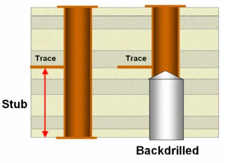
Controlled depth drilling is a specialized manufacturing process used in PCB production to remove unused portions of plated through-hole vias, known as via stubs. These stubs are leftover sections of vias that don’t serve a functional purpose in signal transmission but can cause significant issues in high-speed designs. By drilling out these stubs with precision, controlled depth drilling minimizes signal reflections, reduces noise, and enhances overall performance.
In high-speed PCBs, signals can travel at rates exceeding 10 Gbps. At such speeds, even small imperfections like via stubs can act as antennas, causing signal loss or interference. This makes controlled depth drilling a critical step for engineers looking to push the boundaries of speed while adhering to strict performance standards. Let’s dive deeper into how this technique works and why it’s a game-changer for reducing EMI in PCBs.
How Controlled Depth Drilling Works in High-Speed PCB Design
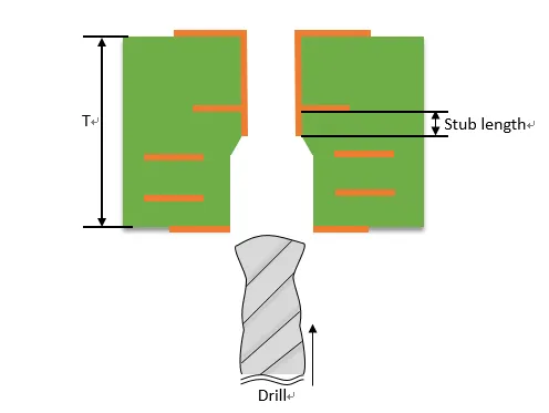
The process of controlled depth drilling involves using a precision drill to remove the non-functional portion of a via after the initial plating process. Vias are conductive pathways that connect different layers of a multi-layer PCB. In high-speed designs, signals often only need to travel through part of the via, leaving the rest as a stub. These stubs can create impedance mismatches, leading to signal reflections that degrade performance.
During back drilling, manufacturers use advanced equipment to drill from the opposite side of the PCB, stopping at a precise depth to eliminate the stub without damaging the functional part of the via. This requires high accuracy, often within tolerances of 0.1 mm, to ensure the integrity of the remaining via structure. The result is a cleaner signal path with reduced distortion, making this technique indispensable for applications like telecommunications and high-performance computing.
Key Steps in the Back Drilling Process
- Design Planning: Engineers identify vias that require back drilling based on signal paths and layer transitions.
- Initial Drilling and Plating: The PCB is manufactured with standard through-hole vias and plated with copper.
- Controlled Depth Drilling: A secondary drilling process removes the unused via stub with precision.
- Inspection: The board is checked to ensure no damage to functional layers and that stubs are fully removed.
Controlled Depth Drilling Benefits for High-Speed PCB Performance
The advantages of controlled depth drilling go beyond just cleaning up signal paths. Here are some of the most significant controlled depth drilling benefits that make it a must-have for high-speed designs:
1. Improved Signal Integrity
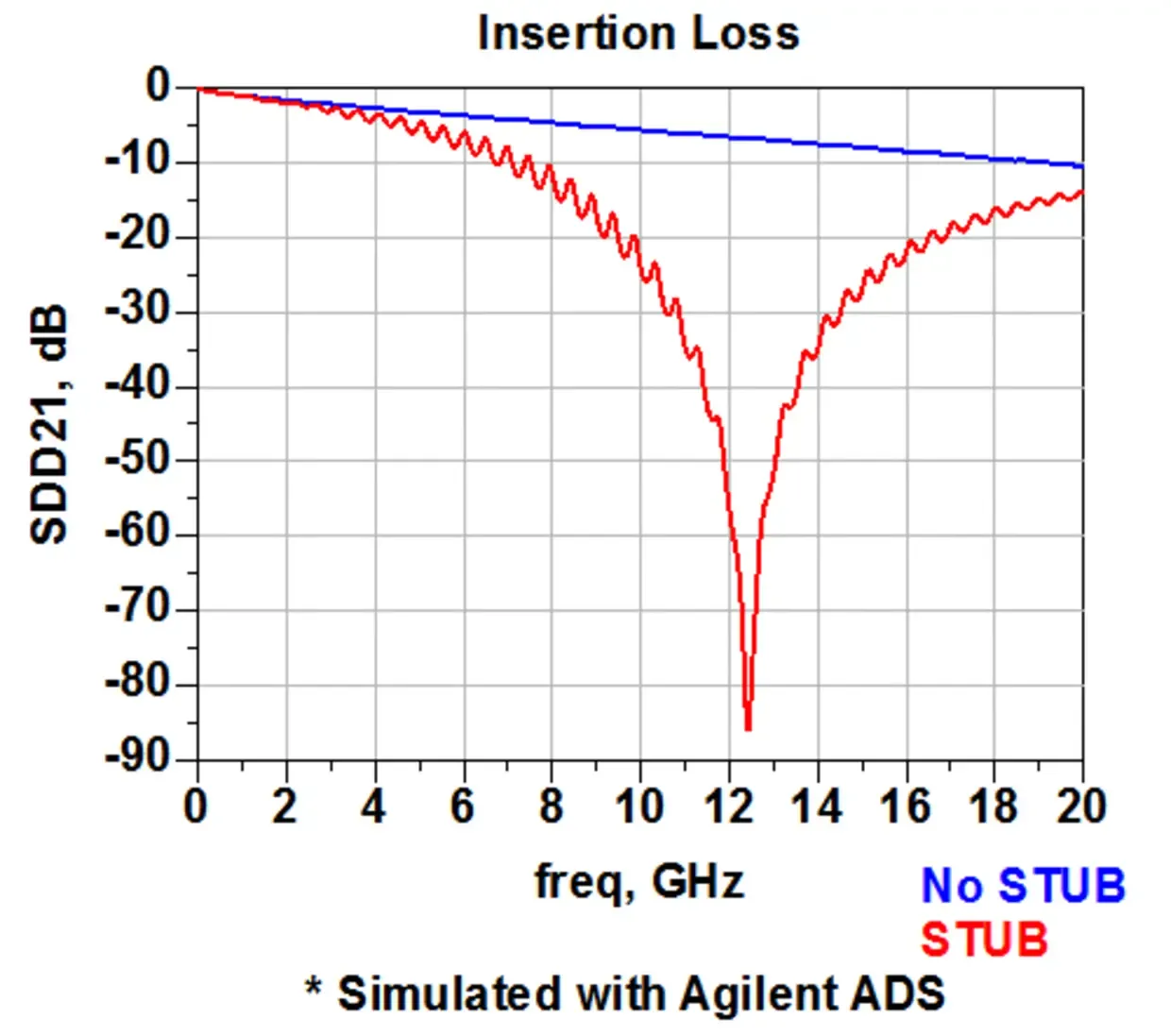
Signal integrity is the cornerstone of high-speed PCB performance. Via stubs can cause signal reflections, leading to data errors or loss. By removing these stubs, controlled depth drilling ensures that signals travel without unnecessary interference. For instance, in a design operating at 25 Gbps, a via stub as short as 0.5 mm can introduce enough reflection to degrade signal quality by up to 20%. Back drilling eliminates this risk, ensuring cleaner waveforms and reliable data transmission.
2. Reduced Electromagnetic Interference (EMI)
Via stubs can act as unintended antennas, radiating or picking up EMI that disrupts nearby signals. This is a major concern in densely packed PCBs where crosstalk is already a challenge. Controlled depth drilling directly contributes to reducing EMI in PCBs by eliminating these stubs, creating a quieter electromagnetic environment for high-speed signals.
3. Better Impedance Control
Impedance mismatches caused by via stubs can alter the electrical characteristics of a signal path, leading to unpredictable performance. Back drilling helps maintain consistent impedance across the via, often keeping it within a tight range like 50 ohms ±5%, which is critical for high-speed applications.
4. Enhanced Design Flexibility
Without the worry of via stubs, engineers have more freedom to design complex multi-layer boards with numerous vias. This flexibility is especially valuable in compact devices where space is limited, and high-speed performance is non-negotiable.
PCB Via Design Guidelines for Optimal Back Drilling
To fully leverage the benefits of controlled depth drilling, it’s essential to follow PCB via design guidelines during the design phase. These best practices ensure that back drilling is both feasible and effective in enhancing performance.
1. Minimize Via Stub Length in Design
During the layout stage, plan signal transitions to occur as close as possible to the top or bottom layers of the PCB. This reduces the length of potential via stubs even before back drilling, making the process more efficient. For example, routing a high-speed signal from layer 1 to layer 3 instead of layer 10 in a 12-layer board minimizes the stub length.
2. Specify Back Drilling Requirements Clearly
Include detailed notes in your design files about which vias require back drilling and the target depth. Clear communication with the manufacturer prevents errors and ensures that only the necessary vias are processed.
3. Use Appropriate Via Sizes
Smaller via diameters can complicate back drilling due to the precision required. Stick to standard via sizes (e.g., 0.3 mm to 0.5 mm) that are compatible with most drilling equipment to avoid manufacturing issues.
4. Avoid Overlapping Vias
Placing vias too close together can make back drilling challenging, as the drill might damage adjacent structures. Maintain a minimum spacing (often 1.5 times the via diameter) to ensure a clean process.
By adhering to these guidelines, you can optimize your PCB for high-speed PCB back drilling and achieve the best possible results in signal performance.
Signal Integrity Improvement Techniques Beyond Back Drilling
While controlled depth drilling is a powerful tool, it’s just one of many signal integrity improvement techniques available to PCB designers. Combining back drilling with other strategies can further enhance performance in high-speed designs.
1. Proper Layer Stackup Design
A well-planned layer stackup minimizes signal crosstalk and ensures consistent impedance. For instance, placing high-speed signal layers between ground planes can shield them from interference, complementing the effects of back drilling.
2. Differential Pair Routing
Routing high-speed signals as differential pairs reduces noise and improves signal integrity. Maintaining equal trace lengths and tight coupling (e.g., spacing of 5 mils for 10 Gbps signals) works hand-in-hand with stub minimization to ensure clean data transmission.
3. Use of Low-Loss Materials
Selecting PCB materials with low dielectric constants (Dk) and low dissipation factors (Df), such as those with Dk values around 3.0, reduces signal loss at high frequencies. This enhances the benefits of controlled depth drilling by ensuring signals travel with minimal attenuation.
Integrating these techniques creates a robust approach to high-speed PCB design, where back drilling plays a central role in maintaining clean signal paths.
Applications of Controlled Depth Drilling in High-Speed Designs
Controlled depth drilling is widely used across industries where high-speed performance is critical. Some key applications include:
- Telecommunications: In 5G infrastructure, where signal speeds often exceed 20 Gbps, back drilling ensures reliable data transfer with minimal latency.
- Data Centers: Servers and networking equipment rely on high-speed PCBs to handle massive data throughput, making stub minimization essential.
- Aerospace and Defense: High-frequency radar and communication systems demand impeccable signal integrity, which back drilling helps achieve.
- Consumer Electronics: Devices like gaming consoles and high-end smartphones benefit from reduced EMI and improved performance through controlled depth drilling.
Challenges and Considerations in Controlled Depth Drilling
While the benefits are clear, controlled depth drilling does come with some challenges that designers and manufacturers must address:
1. Manufacturing Complexity
Back drilling requires specialized equipment and skilled operators to achieve the necessary precision. This can increase production costs, especially for small runs or prototypes.
2. Design Constraints
Not all vias can be back drilled due to layout or spacing limitations. Engineers must carefully plan their designs to accommodate this process without compromising other aspects of the board.
3. Testing and Validation
After back drilling, thorough testing is needed to confirm that no damage has occurred to functional vias and that signal performance meets expectations. Tools like time-domain reflectometry (TDR) can measure impedance and verify the effectiveness of stub removal.
Despite these challenges, the performance gains often outweigh the added complexity, especially for cutting-edge applications.
Conclusion: Why Controlled Depth Drilling Is Essential for High-Speed PCBs
As electronic devices continue to demand faster data rates and higher reliability, techniques like controlled depth drilling are no longer optional—they’re essential. By minimizing via stubs, this process delivers significant controlled depth drilling benefits, including improved signal integrity, reduced EMI, and better impedance control. Following PCB via design guidelines and integrating other signal integrity improvement techniques ensures that your high-speed designs perform at their peak.


