 ALLPCB


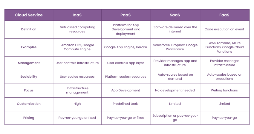
If you're searching for the best cloud PCB software to streamline your design process, you're in the right place. With the rise of remote work and collaborative engineering, cloud-based electronic design automation (EDA) tools have become essential for PCB designers. In this detailed guide, we'll provide a cloud EDA comparison, review popular online PCB design tools, and break down key cloud PCB software features to help you make an informed decision. Whether you're a hobbyist or a professional engineer, this post will guide you through the options and considerations for choosing the perfect cloud-based solution for your needs.
Why Choose Cloud PCB Software?
Cloud-based PCB design tools have transformed the way engineers work by offering flexibility, accessibility, and collaboration. Unlike traditional desktop software that requires powerful hardware and local installations, cloud solutions allow you to design circuits from any device with an internet connection. This means you can work from home, the office, or even on the go without worrying about software compatibility or file transfers.
Additionally, cloud platforms often include real-time collaboration features, enabling teams to work together seamlessly, even across different time zones. Automatic updates ensure you're always using the latest version of the software, and cloud storage reduces the risk of losing your designs due to hardware failures. With these benefits in mind, let’s dive into the key factors to consider when selecting a cloud PCB tool.
Key Features to Look for in Cloud PCB Software
Before we compare specific tools, it’s important to understand the essential cloud PCB software features that can impact your workflow. Here are the main aspects to evaluate:
- User Interface and Ease of Use: A clean, intuitive interface can save hours of learning time. Look for software with drag-and-drop functionality and customizable workspaces to match your design style.
- Collaboration Tools: Real-time collaboration is a cornerstone of cloud solutions. Ensure the software supports multiple users editing the same project simultaneously and offers version control to track changes.
- Library and Component Access: Comprehensive libraries with pre-built components (resistors, capacitors, ICs) are crucial. Some platforms also allow you to import custom components or integrate with external databases for up-to-date parts.
- Simulation and Analysis: Advanced tools offer built-in simulation for testing signal integrity and thermal performance. For example, the ability to analyze impedance mismatches at high frequencies (e.g., 50 ohms for RF designs) can prevent costly errors.
- Integration with Manufacturing: Seamless export of Gerber files, BOM (Bill of Materials), and direct integration with fabrication services can speed up the transition from design to production.
- Pricing and Scalability: Many cloud tools offer subscription-based pricing, with free tiers for beginners and premium plans for professionals. Check if the software scales with your needs as your projects grow in complexity.
- Security and Data Protection: Since your designs are stored online, ensure the platform uses robust encryption and offers backup options to protect your intellectual property.
By prioritizing these features based on your specific requirements, you can narrow down the options and find a tool that fits your workflow.
Cloud EDA Comparison: What Sets Tools Apart?
In this cloud EDA comparison, we’ll explore how different platforms stack up in terms of functionality and user experience. While we won’t mention specific brand names, we’ll categorize tools into common types based on their target audience and capabilities. This will help you understand which type of software aligns with your goals.
1. Beginner-Friendly Cloud Tools
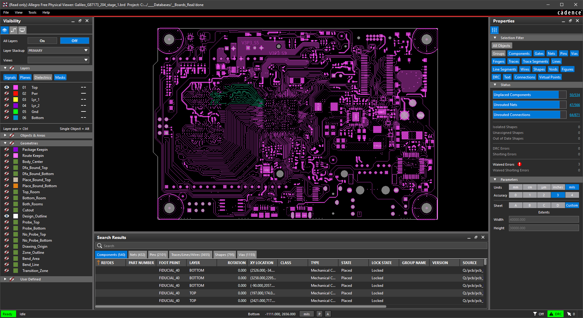
These platforms are ideal for hobbyists, students, or small-scale projects. They typically offer a free tier with basic schematic capture and layout tools. While they may lack advanced simulation features, they often include extensive tutorials and community support to help new users get started. For instance, a beginner tool might limit designs to 2-4 layers, which is sufficient for simple circuits like LED drivers operating at low frequencies (e.g., 1-10 kHz).
Pros: Easy to learn, cost-effective, and lightweight. Cons: Limited features for complex designs, such as high-speed signal routing with controlled impedance (e.g., 100 ohms for differential pairs).
2. Mid-Range Collaborative Platforms
Targeted at small teams or freelance engineers, mid-range cloud tools balance affordability with more advanced features. They often support real-time collaboration, allowing multiple users to edit a design simultaneously. Some platforms in this category also provide basic signal integrity analysis, which can detect issues like crosstalk in designs operating at moderate speeds (e.g., 100 MHz).
Pros: Affordable for small businesses, good collaboration features. Cons: May not handle extremely complex designs with dozens of layers or ultra-high-speed signals (e.g., 1 GHz or above).
3. Enterprise-Grade Cloud Solutions
For large organizations or projects requiring high-performance designs, enterprise-grade tools offer comprehensive features. These include advanced simulation for thermal and electromagnetic analysis, support for multi-board systems, and integration with supply chain management. Such tools are essential for designs with strict requirements, like maintaining signal integrity at 2.5 GHz for high-speed communication protocols.
Pros: Robust feature set, ideal for complex projects. Cons: Higher cost, steeper learning curve for new users.
Online PCB Design Tools Review: What Users Value Most
In this online PCB design tools review, we’ve gathered insights from user feedback and industry trends to highlight what engineers appreciate and where challenges lie. While specific tools vary, common themes emerge across platforms.
User-Friendly Design Experience
Many users prioritize software that minimizes the learning curve. For example, tools with pre-designed templates for common circuits (like power supplies with 5V output) allow users to start designing immediately. A clutter-free interface with tooltips for functions like trace routing or via placement also enhances productivity.
Collaboration and Remote Access
Engineers working in distributed teams often highlight the importance of cloud-based collaboration. The ability to share a design instantly and see live updates from colleagues—such as adjusting a trace width from 10 mils to 15 mils for current capacity—saves time and reduces errors.
Reliability and Performance
Some users report occasional lags or downtime with cloud tools, especially during peak usage. While most platforms aim for 99.9% uptime, it’s worth checking user reviews for reliability. Additionally, ensure the tool can handle your design’s complexity, such as routing for a 6-layer board with 500+ components.
Cost vs. Value
Pricing is a frequent discussion point. Free or low-cost tools are great for small projects, but users often find that investing in a paid plan (e.g., $10-50 per month) unlocks critical features like auto-routing or advanced DRC (Design Rule Check) for ensuring manufacturability.
Image Placement Suggestion: Place an image here of a team collaborating on a PCB design via a cloud platform, with multiple screens showing the same project. ALT Text: "Team collaboration using cloud PCB software"
How to Choose the Best Cloud PCB Software for Your Needs
Finding the best cloud PCB software depends on your specific use case. Here’s a step-by-step guide to help you decide:
- Define Your Project Requirements: Are you designing a simple 2-layer board for a hobby project, or a complex 10-layer board for industrial use? List must-have features like layer support or simulation capabilities.
- Set a Budget: Determine how much you’re willing to spend. Free tools might suffice for basic designs, while professional projects may justify a subscription of $100 or more per month.
- Test Accessibility: Since cloud tools rely on internet connectivity, ensure the platform works smoothly on your devices and network. Look for offline modes if you work in areas with unstable connections.
- Evaluate Support and Community: A strong user community or responsive customer support can be a lifesaver when troubleshooting issues like incorrect via stitching on a ground plane.
- Try Before You Buy: Most cloud tools offer free trials or limited versions. Test a few platforms by creating a small design, such as a basic amplifier circuit with a 9V power input, to see which feels most comfortable.
By following these steps, you can confidently select a tool that matches both your technical and financial needs.
Benefits of Using Cloud PCB Software with ALLPCB Services
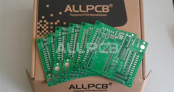
Pairing your chosen cloud PCB software with a reliable manufacturing service like ALLPCB can streamline your workflow from design to production. Our platform supports direct file uploads from most cloud tools, ensuring your Gerber files and BOMs are ready for fabrication without compatibility issues. With fast turnaround times and quality assurance, ALLPCB helps bring your designs to life, whether you’re prototyping a small batch or scaling up to mass production.
For instance, if your design requires precise trace widths of 6 mils for high-current paths, our manufacturing process ensures accuracy down to the smallest detail. Plus, our team can assist with design reviews to catch potential issues before production, saving you time and cost.
Common Challenges with Cloud PCB Software and How to Overcome Them
While cloud-based tools offer many advantages, they come with potential challenges. Here’s how to address them:
- Internet Dependency: Without a stable connection, access to your designs can be interrupted. Look for tools with offline capabilities or maintain local backups of critical files.
- Data Security: Store sensitive designs on platforms with strong encryption and two-factor authentication. Avoid sharing access credentials with unauthorized users.
- Learning Curve: Some advanced tools may feel overwhelming at first. Take advantage of built-in tutorials or online resources to master features like differential pair routing for high-speed signals (e.g., 500 MHz).
By anticipating these issues and planning ahead, you can enjoy the benefits of cloud PCB design without the drawbacks.
Future Trends in Cloud PCB Design Tools
The world of cloud EDA is evolving rapidly. Emerging trends include the integration of artificial intelligence for automated routing and component placement, which can reduce design time for complex boards by up to 30%. Additionally, enhanced simulation capabilities are being developed to predict real-world performance more accurately, such as thermal dissipation in designs with power components dissipating 5W or more.
Another exciting development is the push toward greater interoperability between design tools and manufacturing platforms. This means you’ll be able to get instant quotes and design feedback directly within your cloud software, further bridging the gap between concept and creation.
Conclusion: Make an Informed Choice for Your PCB Design Journey
Selecting the right cloud PCB software is a critical decision that can impact the efficiency and success of your projects. By understanding key cloud PCB software features, conducting a thorough cloud EDA comparison, and reviewing online PCB design tools, you’re well-equipped to find the best cloud PCB software for your needs. Remember to align your choice with your project complexity, budget, and collaboration requirements.
At ALLPCB, we’re committed to supporting your design journey by offering seamless manufacturing solutions that complement your cloud-based workflow. Whether you’re a beginner or a seasoned engineer, the right tools and partnerships can help turn your ideas into reality with precision and speed. Start exploring your options today, and take the first step toward smarter, more efficient PCB design.


