 ALLPCB


When designing a printed circuit board (PCB), one of the most critical factors to consider is trace spacing. But how do you calculate the maximum trace spacing to ensure safety, performance, and reliability? In this guide, we’ll walk you through a practical approach to determining trace spacing using tools like a trace spacing calculator, PCB clearance calculator, and PCB creepage calculator. Whether you're a beginner or a seasoned engineer, this blog will provide actionable steps and insights to help you design better PCBs with the right spacing for your traces.
Trace spacing is the distance between two conductive paths on a PCB. Getting it right prevents electrical issues like short circuits, arcing, and interference. By using an online trace spacing tool or following industry standards, you can ensure your design meets safety and performance requirements. Let’s dive into the details of calculating maximum trace spacing with a step-by-step approach.
Why Trace Spacing Matters in PCB Design
Trace spacing is more than just a design detail; it’s a fundamental aspect of ensuring your PCB works as intended. If traces are too close, you risk electrical interference, crosstalk, or even catastrophic failures like arcing in high-voltage applications. On the other hand, spacing traces too far apart can waste valuable board space, making your design less efficient.
The spacing between traces directly impacts:
- Safety: Proper spacing prevents short circuits and arcing, especially in high-voltage designs where safety standards are strict.
- Signal Integrity: Adequate spacing reduces crosstalk and electromagnetic interference (EMI), ensuring signals remain clear and reliable.
- Manufacturing Feasibility: Spacing must align with the capabilities of your fabrication process to avoid production errors.
For these reasons, calculating maximum trace spacing isn’t just a suggestion—it’s a necessity. Tools like a PCB clearance calculator or PCB creepage calculator can simplify this process by providing precise measurements based on your design parameters.
Understanding Key Terms: Clearance and Creepage
Before diving into calculations, let’s clarify two essential concepts: clearance and creepage. These terms are often used when discussing trace spacing and are critical for ensuring safety in PCB design.
- Clearance: This is the shortest distance through the air between two conductive parts. It’s crucial for preventing arcing in high-voltage designs. For example, a clearance of 0.6 mm might be required for a 50V DC circuit to avoid breakdown under standard conditions.
- Creepage: This refers to the shortest distance along the surface of an insulating material between two conductive parts. Creepage is important for preventing surface tracking, where current flows over the board’s surface due to contamination or moisture. A typical creepage distance for a 100V application might be 1.25 mm, depending on the material and environment.
Both clearance and creepage distances depend on factors like voltage levels, environmental conditions, and the insulating material used. A PCB creepage calculator can help determine these values based on industry standards like IPC-2221 or IEC 60950.
Factors Affecting Maximum Trace Spacing
Calculating maximum trace spacing isn’t a one-size-fits-all process. Several factors influence the spacing requirements for your PCB design:
- Voltage Levels: Higher voltages require larger spacing to prevent arcing. For instance, a 500V circuit might need a clearance of 6 mm, while a 5V circuit may only need 0.2 mm.
- Environmental Conditions: Humidity, dust, and altitude can affect how electricity behaves. Designs for harsh environments often need greater spacing to account for potential contamination.
- Board Material: The dielectric properties of your PCB material (like FR-4) impact creepage distances. Materials with lower comparative tracking index (CTI) values require larger creepage distances.
- Application Type: High-speed digital circuits may need tighter spacing to minimize signal delay, while power electronics demand larger spacing for safety.
- Manufacturing Constraints: Your fabricator’s capabilities, such as minimum trace spacing, also play a role. Standard processes might support 0.15 mm spacing, while advanced processes can go as low as 0.1 mm.
Understanding these factors is the first step to calculating accurate trace spacing. An online trace spacing tool can factor in many of these variables to give you a reliable starting point.
Step-by-Step Guide to Calculating Maximum Trace Spacing
Now that we’ve covered the basics, let’s walk through a practical approach to calculating maximum trace spacing. This method combines manual calculations with the use of digital tools for accuracy.
Step 1: Determine Voltage Levels
Start by identifying the voltage levels in your design. Are you working with low-voltage signals (below 50V) or high-voltage power circuits (above 300V)? The voltage directly impacts the required clearance and creepage distances. For example, a 100V DC circuit might require a minimum clearance of 1.5 mm based on common safety standards.
Step 2: Check Industry Standards
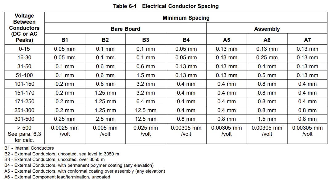
Refer to established standards like IPC-2221, which provides guidelines for trace spacing based on voltage, environment, and application. These standards often include tables that list minimum spacing for different voltage ranges. For instance, IPC-2221 suggests a clearance of 2.5 mm for voltages between 101-150V in uncoated PCBs at sea level.
Step 3: Use a Trace Spacing Calculator
For quick and accurate results, use a trace spacing calculator or PCB clearance calculator. These tools allow you to input parameters like voltage, board material, and environmental conditions to get recommended spacing values. Many online trace spacing tools are available for free and can save you time while ensuring compliance with standards.
Step 4: Account for Creepage with a PCB Creepage Calculator
Creepage distances are often larger than clearance due to the risk of surface tracking. Use a PCB creepage calculator to determine the minimum surface distance between traces. For a 200V application on an FR-4 board in a moderately polluted environment, you might need a creepage distance of 3.2 mm.
Step 5: Adjust for Manufacturing Limits
Finally, check with your PCB manufacturer to ensure your calculated spacing aligns with their capabilities. If your design requires a minimum spacing of 0.2 mm but your fabricator can only achieve 0.25 mm, you’ll need to adjust your layout accordingly.
By following these steps, you can calculate the maximum trace spacing that balances safety, performance, and manufacturability.
Tools for Simplifying Trace Spacing Calculations
Manual calculations can be time-consuming and prone to error, especially for complex designs. Thankfully, several digital tools can streamline the process:
- Online Trace Spacing Tool: These web-based calculators let you input design parameters and instantly get recommended spacing values. They often incorporate industry standards, making them a reliable choice for quick checks.
- PCB Clearance Calculator: Focused on air gap distances, these tools help ensure your design avoids arcing risks in high-voltage applications.
- PCB Creepage Calculator: These calculators specialize in surface distances, factoring in material properties and environmental conditions to provide accurate creepage values.
Using these tools, you can avoid guesswork and ensure your PCB design meets safety and performance requirements. Many of these tools are freely accessible and user-friendly, even for beginners.
Practical Examples of Trace Spacing Calculations
Let’s look at two practical examples to see how trace spacing calculations work in real-world scenarios.
Example 1: Low-Voltage Digital Circuit
Suppose you’re designing a 5V digital circuit for a microcontroller board. Using an online trace spacing tool, you input the voltage (5V) and select a standard FR-4 material. The tool suggests a minimum clearance of 0.13 mm based on IPC-2221 standards. Since this is a low-voltage application with minimal risk of arcing, this spacing is sufficient. You also check with your manufacturer, who confirms they can handle spacing down to 0.1 mm, so your design is feasible.
Example 2: High-Voltage Power Supply
For a 400V power supply design, safety is critical. Using a PCB clearance calculator, you determine a minimum clearance of 5 mm to prevent arcing. A PCB creepage calculator suggests a surface distance of 8 mm due to the risk of tracking in a moderately humid environment. After consulting the IPC-2221 standard, you confirm these values align with recommendations for voltages between 301-500V. You adjust your layout to accommodate these larger spacings, ensuring safety and reliability.
These examples show how different applications require tailored approaches to trace spacing. Whether you’re working on low or high-voltage designs, the right tools and standards can guide you to the correct spacing.
Tips for Optimizing Trace Spacing in Your Design
Beyond calculations, here are some practical tips to optimize trace spacing in your PCB layout:
- Group Similar Nets: Keep high-voltage traces away from low-voltage signals to minimize interference and reduce spacing requirements in critical areas.
- Use Ground Planes: A well-designed ground plane can reduce EMI and allow for tighter spacing in digital circuits without sacrificing signal integrity.
- Consider Coating: Applying a conformal coating can reduce creepage requirements by protecting the board from moisture and contamination.
- Simulate Your Design: Use simulation software to test signal integrity and identify potential issues with spacing before finalizing your layout.
These strategies can help you achieve a balance between compact design and reliable performance.
Common Mistakes to Avoid When Calculating Trace Spacing
Even with the best tools, mistakes can happen. Here are some common pitfalls to watch out for:
- Ignoring Voltage Peaks: Don’t base your calculations solely on nominal voltage. Account for transient spikes, which can be much higher and require larger spacing.
- Neglecting Environment: Failing to consider operating conditions like humidity or altitude can lead to insufficient spacing and potential failures.
- Overlooking Standards: Always refer to industry standards like IPC-2221 to ensure your design meets safety and reliability guidelines.
- Assuming Uniform Spacing: Not all traces need the same spacing. High-speed or high-voltage traces often require more space than others.
By being mindful of these errors, you can avoid costly redesigns and ensure your PCB performs as expected.
Conclusion: Mastering Trace Spacing for Better PCB Designs
Calculating maximum trace spacing is a critical step in PCB design that directly impacts safety, performance, and manufacturability. By understanding key concepts like clearance and creepage, considering factors like voltage and environment, and using tools such as a trace spacing calculator, PCB clearance calculator, or PCB creepage calculator, you can achieve accurate and reliable results. Online trace spacing tools make this process even easier, providing quick calculations based on industry standards.
Whether you’re designing a simple low-voltage board or a complex high-voltage power supply, the practical approach outlined in this guide can help you determine the right trace spacing for your needs. With careful planning and the right resources, you’ll create PCB designs that are safe, efficient, and ready for production.
At ALLPCB, we’re committed to supporting your design journey with resources and expertise. Use this guide as a starting point to refine your trace spacing calculations and elevate the quality of your PCB projects.


