 ALLPCB


Are you looking to maximize power density in compact electronics? 2oz copper PCBs are a game-changer for achieving high performance in small form factor designs. These thicker copper layers allow for better current carrying capacity, improved thermal management, and the ability to shrink PCB size without sacrificing reliability. In this blog, we’ll dive deep into how 2oz copper PCBs are transforming compact PCB design, high density PCB layout, and small form factor PCB applications for electrical engineers.
Introduction: The Need for Power Density in Modern Electronics
In today’s fast-paced world of electronics, devices are getting smaller while performance demands are skyrocketing. Think about smartphones, wearables, IoT devices, and automotive electronics—each requires more power and functionality packed into tighter spaces. This is where 2oz copper PCBs come into play, offering a solution for 2oz copper PCB miniaturization and enabling engineers to design cutting-edge products.
As an electrical engineer, you’re likely facing challenges like heat dissipation, current capacity, and space constraints. Standard 1oz copper PCBs often fall short in high-power applications or when trying to achieve a compact PCB design. By upgrading to 2oz copper, you can handle higher currents—up to 4-6 amps per trace compared to 2-3 amps on 1oz copper—while reducing board size. Let’s explore how this technology is revolutionizing high density PCB layout and beyond.
What Are 2oz Copper PCBs and Why Do They Matter?
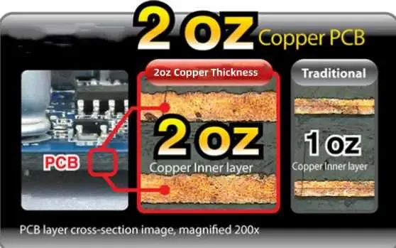
A 2oz copper PCB refers to a printed circuit board with a copper foil thickness of 2 ounces per square foot, equivalent to about 70 micrometers. This is double the thickness of the standard 1oz copper (35 micrometers) used in most general-purpose PCBs. The added thickness means the board can carry more current, dissipate heat better, and provide greater mechanical strength—key factors for small form factor PCB designs.
For electrical engineers working on power electronics or high-current applications, 2oz copper offers significant advantages. For instance, a 10-mil wide trace on a 2oz copper PCB can handle approximately 5 amps at a temperature rise of 10°C, compared to just 2.5 amps on a 1oz board under the same conditions. This makes it ideal for applications like DC-DC converters, motor controllers, and LED lighting systems where power density is critical.
Moreover, the thicker copper reduces trace resistance, lowering voltage drops and improving overall efficiency. In compact PCB design, this means you can use narrower traces without risking overheating, directly supporting 2oz copper PCB miniaturization efforts.
Key Benefits of 2oz Copper PCBs for Compact Electronics
Let’s break down the specific ways 2oz copper PCBs are boosting power density and enabling high density PCB layout in modern electronics.
1. Higher Current Carrying Capacity
One of the biggest advantages of 2oz copper is its ability to handle higher currents. For engineers designing power supplies or battery management systems, this means you can push more power through smaller traces. A typical 2oz copper trace can support up to 50% more current than 1oz copper for the same width, allowing you to shrink board size without compromising performance.
For example, in a compact PCB design for a portable device, you might need to route 4 amps through a trace. With 1oz copper, you’d need a trace width of about 100 mils to keep temperature rise under control. Switch to 2oz copper, and that width drops to around 60 mils—saving valuable board space.
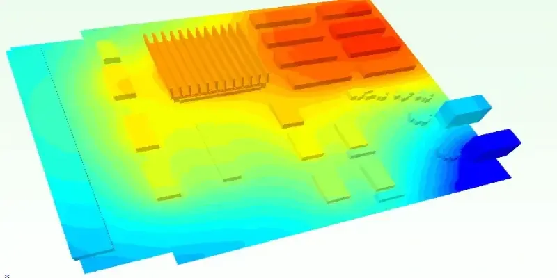
2. Superior Thermal Management
Heat is the enemy of compact electronics. As components get closer together in a high density PCB layout, thermal issues become more pronounced. 2oz copper PCBs excel in dissipating heat due to their thicker conductive layer, which acts as a better heat sink. This reduces the risk of hot spots and extends the lifespan of components.
In a real-world scenario, consider a small form factor PCB for an automotive control unit. With high-power components packed tightly, a 2oz copper layer can reduce thermal resistance by up to 30%, ensuring stable operation even under harsh conditions.
3. Enhanced Mechanical Strength
Thicker copper layers add durability to PCBs, which is crucial for applications where boards face mechanical stress or vibration. In compact electronics like drones or handheld devices, 2oz copper provides better resistance to cracking at connector points or during assembly, ensuring reliability in small form factor PCB designs.
4. Support for Miniaturization
2oz copper PCB miniaturization is at the heart of modern electronics. By allowing narrower traces and tighter spacing without sacrificing current capacity, these boards enable engineers to fit more functionality into less space. This is especially important for high density PCB layout in devices like smartwatches, where every square millimeter counts.
Applications of 2oz Copper PCBs in Compact Electronics
So, where are 2oz copper PCBs making the biggest impact? Here are some key areas where electrical engineers are leveraging this technology for compact PCB design and beyond.
1. Power Electronics
In power supplies, inverters, and converters, 2oz copper PCBs handle high currents and voltages with ease. For instance, a buck converter designed for a laptop charger might use 2oz copper to manage 5-10 amps of current while keeping the board size under 50x50 mm. This directly supports small form factor PCB goals.
2. Automotive Systems
Modern vehicles rely on compact electronics for everything from engine control to infotainment. 2oz copper PCBs are used in ECUs (Electronic Control Units) to manage power distribution efficiently while fitting into tight spaces. Their ability to handle temperature swings and vibrations makes them a top choice for automotive high density PCB layout.
3. IoT and Wearable Devices
The Internet of Things (IoT) and wearables demand ultra-compact designs with reliable power delivery. A fitness tracker, for example, might use a 2oz copper PCB to power sensors and Bluetooth modules in a board smaller than 30x20 mm. This showcases how 2oz copper PCB miniaturization drives innovation in consumer electronics.
Design Considerations for 2oz Copper PCBs
While 2oz copper PCBs offer incredible benefits, they come with unique design challenges. Here’s what electrical engineers need to keep in mind when integrating them into compact PCB design.
1. Trace Width and Spacing
Although 2oz copper allows narrower traces for the same current, you still need to balance this with manufacturing capabilities. Most PCB fabricators recommend a minimum trace width of 6 mils and spacing of 6 mils for 2oz copper to avoid issues like under-etching. Check with your manufacturer to ensure your high density PCB layout meets their tolerances.
2. Cost Implications
Thicker copper means higher material costs. A 2oz copper PCB can cost 20-30% more than a 1oz board for the same dimensions. However, the space savings and performance gains often justify the expense, especially in small form factor PCB projects where size reduction is critical.
3. Thermal Vias and Layer Stackup
To maximize heat dissipation, incorporate thermal vias in your design to transfer heat from components to the copper layer. Additionally, consider a multilayer stackup if your compact PCB design requires both high power and signal integrity. For example, a 4-layer board with 2oz copper on power layers and 1oz on signal layers can optimize performance.
4. Signal Integrity
In high-frequency applications, thicker copper can slightly increase capacitance between traces, potentially affecting signal integrity. Keep trace lengths short and use proper impedance matching (aim for 50 ohms for most RF designs) to mitigate this in high density PCB layout.
Challenges and Solutions in 2oz Copper PCB Miniaturization
Miniaturizing PCBs with 2oz copper isn’t without hurdles. Let’s look at common challenges and practical solutions for electrical engineers.
Challenge 1: Manufacturing Limitations
Not all PCB manufacturers can handle 2oz copper with tight tolerances required for compact designs. Solution: Partner with a reputable fabricator experienced in heavy copper PCBs. Many online services now offer detailed specs for 2oz copper boards, ensuring your small form factor PCB is produced accurately.
Challenge 2: Increased Weight
Thicker copper adds weight, which can be an issue in ultra-light devices like drones. Solution: Use 2oz copper only on power layers or critical areas, combining it with 1oz copper elsewhere to balance weight and performance.
Challenge 3: Assembly Complexity
Thicker copper can make soldering more challenging due to higher heat requirements. Solution: Adjust your reflow profile to account for the thermal mass of 2oz copper, ensuring components are mounted securely without damage.
Future Trends: Where 2oz Copper PCBs Are Heading
The push for smaller, more powerful electronics isn’t slowing down. As devices continue to shrink, 2oz copper PCBs will play an even bigger role in 2oz copper PCB miniaturization. Emerging trends include combining 2oz copper with High-Density Interconnect (HDI) technology for even tighter layouts, and integrating advanced materials like ceramic substrates for better thermal performance.
For electrical engineers, staying ahead means experimenting with multilayer designs and leveraging simulation tools to optimize trace layouts. Software like Altium or KiCad can help model current density and heat dissipation before fabrication, ensuring your high density PCB layout performs as expected.
Conclusion: Power Up with 2oz Copper PCBs
2oz copper PCBs are revolutionizing compact electronics by boosting power density, improving thermal management, and enabling 2oz copper PCB miniaturization. For electrical engineers, they offer a reliable way to meet the demands of modern devices through compact PCB design, high density PCB layout, and small form factor PCB applications. Whether you’re working on power electronics, automotive systems, or IoT gadgets, upgrading to 2oz copper can give your designs the edge they need.
Ready to take your next project to the next level? Start by evaluating your current PCB needs—could 2oz copper solve your space or power challenges? Partner with a trusted manufacturer, optimize your layout for thermal and current demands, and watch as your compact designs achieve new heights of performance.


