 ALLPCB


When designing a printed circuit board (PCB) for high-current applications, one of the most critical factors to consider is the trace width. Using a calculator to determine trace width is a great starting point, but achieving optimal performance and reliability goes beyond simple calculations. Factors like thermal management, copper weight, and current capacity play a huge role in preventing issues such as PCB trace overheating. In this comprehensive guide, we’ll explore how to optimize maximum line width for high-current PCB design, diving deep into practical strategies for ensuring your board can handle the load safely and efficiently.
Why Trace Width Matters in High-Current PCB Design
In high-current PCB design, trace width directly impacts how much current a board can carry without overheating or failing. A trace that’s too narrow for the current it carries will heat up, potentially leading to performance issues, delamination, or even complete failure of the board. On the other hand, a trace that’s too wide can waste valuable board space and increase manufacturing costs. Striking the right balance is key to creating a reliable and cost-effective design.
Optimizing trace width for high current isn’t just about meeting the minimum requirements. It’s about understanding the interplay between current capacity, heat dissipation, and the physical properties of the materials used. Let’s break down the essential elements of this process to help you design better PCBs for demanding applications.
Understanding PCB Trace Width for High Current
The width of a PCB trace determines its ability to carry current without excessive heat buildup. A wider trace has a larger cross-sectional area, which reduces electrical resistance and allows more current to flow. However, the relationship isn’t linear—doubling the width doesn’t double the current capacity due to factors like heat dissipation and skin effect at higher frequencies.
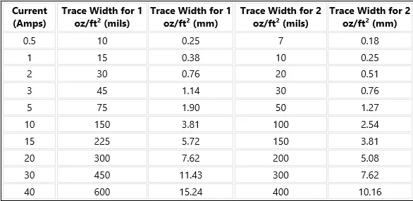
For high-current designs, traces often need to handle currents of 5A, 10A, or even higher. According to industry standards like IPC-2221, a widely used guideline for PCB design, the trace width for a 10A current on a 1 oz/ft2 copper layer (approximately 35 μm thick) should be around 200 mils (5.08 mm) for a temperature rise of 10°C above ambient. If the temperature rise limit is stricter, say 5°C, the width must increase further. These values are starting points, but real-world designs often require adjustments based on specific conditions like board layering, ambient temperature, and airflow.
Factors Affecting Maximum Current Capacity in PCBs
The maximum current capacity of a PCB trace depends on several factors beyond just width. Let’s explore the most critical ones to help you design for reliability and performance.
1. Copper Weight vs Trace Width
Copper weight, often measured in ounces per square foot (oz/ft2), determines the thickness of the copper layer on the PCB. Common weights are 1 oz/ft2 (35 μm thick) and 2 oz/ft2 (70 μm thick), though heavier options like 3 oz/ft2 or more are used for extreme high-current applications. A thicker copper layer increases the cross-sectional area of the trace, allowing it to carry more current for the same width.
For example, a 100-mil (2.54 mm) wide trace on a 1 oz/ft2 copper layer might safely carry 5A with a 10°C temperature rise. On a 2 oz/ft2 layer, the same width could handle closer to 8A under similar conditions. Choosing the right copper weight is a balancing act—thicker copper improves current capacity but increases manufacturing costs and can complicate etching processes for fine traces.
2. Trace Length and Resistance
Longer traces have higher resistance, which leads to greater voltage drops and heat generation. If you’re designing for high current, minimize trace length wherever possible. For instance, a 10-inch (254 mm) trace carrying 10A on a 1 oz/ft2 copper layer could experience a voltage drop of around 0.05V, depending on the width. This might seem small, but in precision circuits, even minor drops can affect performance.
3. Ambient Temperature and Environment
The operating environment of your PCB plays a big role in current capacity. A board operating in a hot environment (e.g., 50°C ambient temperature) will have less capacity to handle heat compared to one in a cooler setting (e.g., 25°C). If your design will be enclosed in a case with poor ventilation, you’ll need wider traces or heavier copper to compensate for reduced heat dissipation.
Preventing PCB Trace Overheating: Key Strategies
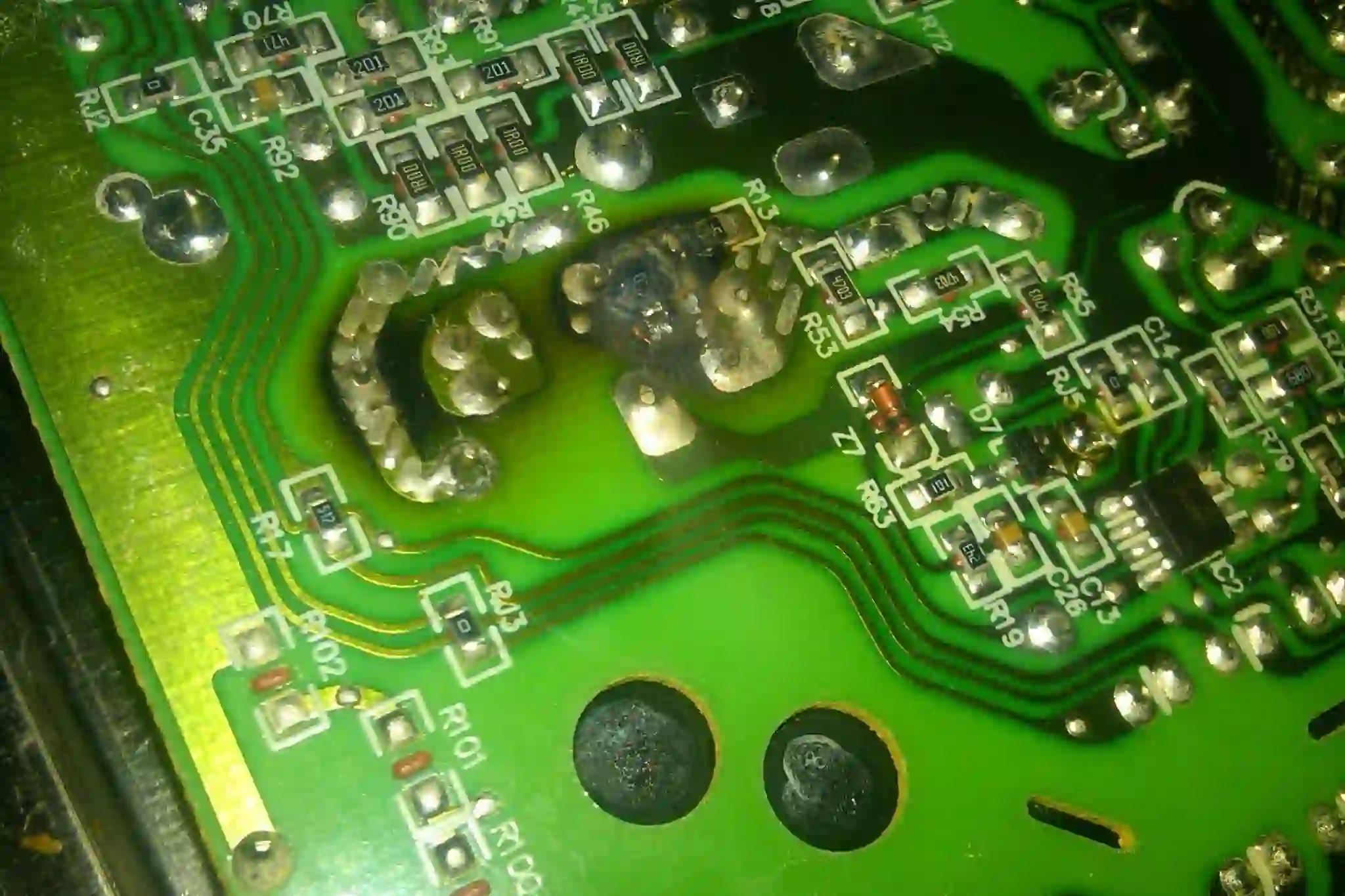
Overheating is one of the most common causes of PCB failure in high-current designs. When a trace overheats, it can degrade the board material, cause solder joints to fail, or even start a fire in extreme cases. Here are proven strategies to keep temperatures under control.
1. Use Wider Traces Where Possible
As a rule of thumb, increasing trace width is the simplest way to reduce heat. Wider traces lower resistance and spread heat over a larger area. If board space is limited, consider splitting high-current paths into multiple parallel traces to achieve the same effect without sacrificing too much real estate.
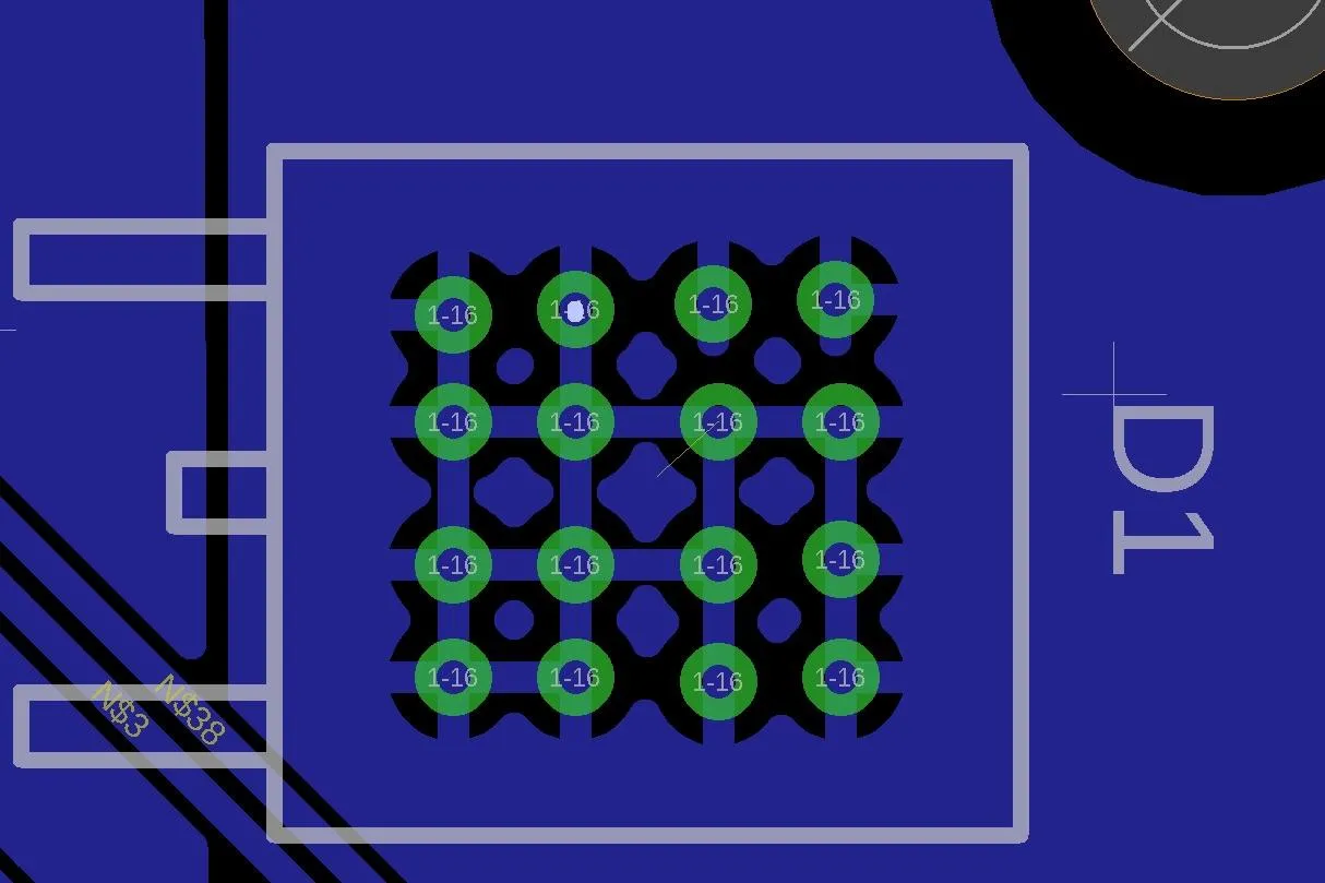
2. Incorporate Thermal Vias
Thermal vias are small holes filled or plated with conductive material that transfer heat from the trace to other layers or a heat sink. For high-current traces, adding thermal vias near hot spots can significantly reduce temperature rise. For example, a study on thermal management showed that adding just 10 thermal vias under a high-current trace can reduce its temperature by up to 15°C.
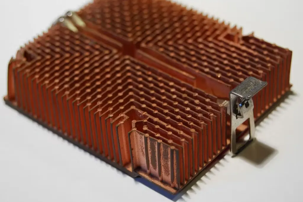
3. Opt for Heavier Copper Layers
As discussed earlier, heavier copper weights allow traces to carry more current with less heat buildup. For applications like power supplies or motor controllers, using 2 oz/ft2 or 3 oz/ft2 copper can make a big difference in thermal performance.
Thermal Management in PCB Design: Best Practices
Effective thermal management in PCB design goes hand-in-hand with optimizing trace width for high current. Without proper heat dissipation, even the widest traces can overheat under heavy loads. Here are some best practices to integrate into your design process.
1. Add Heat Sinks or Copper Pour Areas
Heat sinks are external components that absorb and dissipate heat from the PCB. For traces carrying high current, connecting them to large copper pour areas (also called copper fills) on the board can act as a built-in heat sink. These areas increase the surface area for heat dissipation, lowering the overall temperature of the trace.
2. Optimize Board Layering
In multilayer PCBs, high-current traces can benefit from being placed on outer layers where heat can dissipate more easily into the air. If inner layers are unavoidable, ensure there are enough thermal vias to connect the trace to outer layers or heat-dissipating components.
3. Improve Airflow and Enclosure Design
If your PCB will operate in an enclosed space, design the enclosure with ventilation holes or fans to improve airflow. Better airflow can reduce the ambient temperature around the board, allowing traces to carry more current without overheating. For example, a fan providing 50 CFM (cubic feet per minute) of airflow can lower board temperatures by 10-20°C in a confined space.
Going Beyond the Calculator: Fine-Tuning Your Design
While online calculators and standards like IPC-2221 provide a solid foundation for determining trace width, they often assume ideal conditions that don’t match real-world scenarios. Here’s how to fine-tune your design for maximum reliability.
1. Account for Temperature Rise Limits
Most calculators allow you to input a desired temperature rise (e.g., 10°C or 20°C above ambient). However, the acceptable rise depends on your application. For automotive or industrial environments, a lower temperature rise (5-10°C) might be necessary to ensure long-term reliability. Adjust trace width and copper weight accordingly.
2. Simulate Thermal Performance
Modern PCB design software often includes thermal simulation tools that model heat distribution across your board. Running a simulation can reveal hot spots you might miss with a calculator. For instance, a simulation might show that a trace near a high-power component needs to be 20% wider than calculated to avoid overheating.
3. Test Prototypes Under Load
Before finalizing your design, build and test prototypes under real operating conditions. Use an infrared camera to measure trace temperatures while the board carries its maximum current. If a trace exceeds safe temperature limits (typically 105°C for standard FR-4 material), increase its width or improve thermal management.
Common Mistakes to Avoid in High-Current PCB Design
Even experienced engineers can make mistakes when designing for high current. Here are some pitfalls to watch out for.
1. Underestimating Current Requirements
Always design with a safety margin. If your circuit is expected to carry 10A continuously, design for at least 12-15A to account for spikes or unexpected loads. Underestimating current can lead to overheating and premature failure.
2. Ignoring Voltage Drops
In high-current designs, even small voltage drops can cause problems. Calculate the resistance of your traces and ensure the voltage drop won’t affect downstream components. For a 10A trace with a resistance of 5 mΩ, the voltage drop would be 0.05V—a small but potentially significant loss in low-voltage systems.
3. Neglecting Thermal Expansion
High temperatures cause materials to expand, which can stress solder joints and traces. Over time, this thermal cycling can lead to cracks or failures. Use materials with good thermal stability and design with expansion in mind, especially for traces that will experience frequent heating and cooling.
Conclusion: Mastering High-Current PCB Design
Optimizing trace width for high-current PCB design is a complex but essential task. While calculators provide a useful starting point, truly reliable designs require a deeper understanding of factors like copper weight, thermal management, and environmental conditions. By following the strategies outlined in this guide—using wider traces, incorporating thermal vias, choosing the right copper weight, and simulating performance—you can prevent PCB trace overheating and ensure your board performs flawlessly under load.
Designing for maximum current capacity in PCBs isn’t just about meeting specs; it’s about building boards that last. With careful planning and attention to detail, you can create high-current designs that are both efficient and robust, ready to power the most demanding applications.


