 ALLPCB


When it comes to designing and manufacturing printed circuit boards (PCBs), breakaway tabs play a vital role in panelization and depanelization processes. While FR-4 has long been the standard material for PCBs due to its affordability and versatility, advanced PCB materials like ceramics and Teflon are gaining traction in high-performance applications. These materials bring unique challenges and considerations for breakaway tab design and depanelization. In this blog, we’ll explore how breakaway tabs function with advanced PCB materials, focusing on material properties, design tips, and manufacturing techniques for optimal results. Whether you’re working on ceramic PCB breakaway tabs or Teflon PCB depaneling, this guide will help you navigate the complexities of high-performance PCB manufacturing.
What Are Breakaway Tabs and Why Do They Matter?
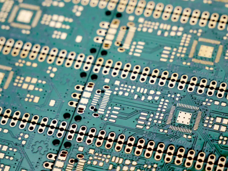
Breakaway tabs are small, strategically placed connectors that hold individual PCBs together in a panel during manufacturing and assembly. These tabs allow multiple boards to be processed as a single unit, improving efficiency and reducing handling errors. Once assembly is complete, the tabs are broken or cut to separate the boards, a process known as depanelization.
For standard FR-4 boards, breakaway tabs are relatively straightforward to design and implement. However, when working with advanced PCB materials, the properties of these materials—such as brittleness in ceramics or flexibility in Teflon—can significantly impact how breakaway tabs perform. Poorly designed tabs can lead to material damage, uneven breaks, or manufacturing delays. Understanding the interplay between PCB material properties and breakaway tabs is essential for ensuring a smooth production process in high-performance PCB manufacturing.
Challenges of Breakaway Tabs with Advanced PCB Materials
Advanced PCB materials are often chosen for their superior electrical, thermal, or mechanical properties. However, these same properties can complicate the use of breakaway tabs. Let’s break down the challenges associated with some common advanced materials.
1. Ceramic PCB Breakaway Tabs: Handling Brittleness
Ceramic PCBs, often made from materials like aluminum oxide or aluminum nitride, are known for their excellent thermal conductivity and high-frequency performance. They are commonly used in applications like LED lighting and power electronics where heat dissipation is critical. However, ceramics are inherently brittle, which poses a significant challenge during depanelization.
With ceramic PCB breakaway tabs, excessive force during separation can cause cracking or chipping, potentially damaging the board or nearby components. To mitigate this, designers must carefully consider tab placement and thickness. For instance, using smaller, thinner tabs with perforations can reduce the force needed to break them. Additionally, scoring lines or V-grooves near the tabs can help guide the break and minimize stress on the material.
2. Teflon PCB Depaneling: Managing Flexibility
Teflon, or polytetrafluoroethylene (PTFE), is a popular choice for high-frequency applications like RF and microwave circuits due to its low dielectric constant and loss tangent. For example, Teflon materials often have a dielectric constant of around 2.1, compared to FR-4’s typical value of 4.5, making them ideal for maintaining signal integrity at frequencies above 1 GHz. However, Teflon’s flexibility and softness create unique challenges during depanelization.
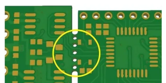
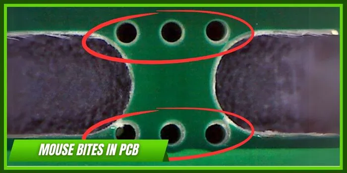
Unlike rigid materials, Teflon can deform or tear when breakaway tabs are separated, leading to uneven edges or damaged boards. To address this, designers often use a combination of breakaway tabs and routing techniques. Pre-cut slots or mouse bites—small perforated holes along the tab—can help control the separation process. Additionally, using a clean, sharp cutting tool during depanelization can prevent material distortion and ensure a smooth finish.
3. Other Advanced PCB Materials: Hybrid and High-Temperature Options
Beyond ceramics and Teflon, other advanced materials like polyimide and high-temperature laminates are used in demanding environments such as aerospace and automotive applications. These materials often combine high thermal stability with unique mechanical properties, which can affect breakaway tab design.
For instance, polyimide is flexible yet durable, requiring tabs that balance strength with ease of separation. High-temperature laminates, on the other hand, may have varying coefficients of thermal expansion, which can lead to stress concentration at tab points during manufacturing. Adjusting tab dimensions and spacing based on the specific material properties is crucial for successful depanelization in these cases.
Key PCB Material Properties Affecting Breakaway Tabs
To design effective breakaway tabs for advanced PCB materials, it’s important to understand the material properties that influence their performance. Here are the primary factors to consider when working on advanced PCB materials depanelization:
- Mechanical Strength: Materials like ceramics have high compressive strength but low tensile strength, making them prone to cracking. Tabs must be designed to minimize bending forces during separation.
- Flexibility: Flexible materials like Teflon require tabs that prevent stretching or tearing. Smaller tabs or perforations can help achieve a clean break.
- Thermal Conductivity: High thermal conductivity in materials like ceramics can lead to heat buildup during cutting or breaking, potentially affecting nearby components. Proper tab spacing can help manage heat dissipation.
- Dielectric Properties: For high-frequency materials like Teflon, maintaining signal integrity near breakaway tabs is critical. Avoid placing tabs near sensitive traces or components to prevent interference.
By tailoring breakaway tab designs to these properties, manufacturers can reduce the risk of damage and improve overall production efficiency in high-performance PCB manufacturing.
Design Best Practices for Breakaway Tabs in Advanced Materials
Creating effective breakaway tabs for advanced PCB materials requires careful planning and attention to detail. Below are some actionable design tips to ensure successful depanelization:
1. Optimize Tab Size and Spacing
The size and spacing of breakaway tabs should be adjusted based on the material’s mechanical properties. For brittle materials like ceramics, use smaller tabs (e.g., 0.5 mm thick) spaced farther apart to reduce stress concentration. For flexible materials like Teflon, slightly larger tabs (e.g., 1 mm thick) with perforations can provide stability during assembly while allowing easy separation.
2. Incorporate Scoring or Mouse Bites
Scoring lines or mouse bites are small perforations or cuts along the breakaway tabs that guide the separation process. These features are especially useful for materials prone to uneven breaking, such as ceramics or Teflon. For instance, a row of 0.3 mm diameter holes spaced 0.5 mm apart can create a clean break line without compromising panel strength during assembly.
3. Consider Tab Placement
Place breakaway tabs away from critical components or high-frequency traces to avoid interference or damage during depanelization. For ceramic PCBs, avoid placing tabs near edges with thin substrates, as these areas are more susceptible to cracking. For Teflon PCBs, ensure tabs are evenly distributed to prevent uneven stress during bending.
4. Test Depanelization Methods
Different materials may require different depanelization techniques. For ceramics, manual breaking with a controlled force tool can prevent cracking. For Teflon, a precision cutting tool or laser depanelization may be more effective in achieving clean edges. Testing various methods on prototype panels can help identify the best approach for a specific material.
Manufacturing Considerations for Advanced PCB Materials Depanelization
In high-performance PCB manufacturing, the depanelization process must be tailored to the material being used. Here are some key considerations to ensure a smooth and damage-free separation:
- Tool Selection: Use tools designed for the specific material. For example, diamond-coated blades are ideal for cutting ceramics due to their hardness, while sharp, fine-edged blades work better for Teflon to avoid tearing.
- Speed and Force Control: Adjust the speed and force of depanelization equipment to match the material’s properties. For brittle materials, slower speeds with minimal force reduce the risk of cracking.
- Environmental Factors: Temperature and humidity can affect material behavior. For instance, Teflon can become more pliable in high temperatures, requiring cooler conditions during depanelization to maintain consistency.
By aligning manufacturing processes with the unique needs of advanced PCB materials, you can achieve cleaner breaks and higher yields during production.
Advantages of Proper Breakaway Tab Design in Advanced Materials
Investing time and effort into breakaway tab design for advanced PCB materials offers several benefits:
- Reduced Material Waste: Properly designed tabs minimize damage during depanelization, reducing the number of defective boards and lowering production costs.
- Improved Efficiency: Streamlined depanelization processes save time during manufacturing, allowing for faster turnaround on high-performance projects.
- Enhanced Product Quality: Clean, precise breaks prevent edge defects that could impact the performance of sensitive applications like RF circuits or power electronics.
Conclusion: Mastering Breakaway Tabs for Advanced PCB Materials
As the demand for high-performance PCB manufacturing continues to grow, understanding the nuances of breakaway tab design for advanced materials like ceramics and Teflon becomes increasingly important. By considering PCB material properties, optimizing tab design, and tailoring depanelization methods, manufacturers can overcome the challenges associated with advanced PCB materials depanelization. Whether you’re working on ceramic PCB breakaway tabs or Teflon PCB depaneling, these strategies will help ensure a seamless production process and high-quality results.
At ALLPCB, we’re committed to supporting engineers and designers in navigating the complexities of modern PCB manufacturing. By applying the insights and best practices shared in this guide, you can achieve better outcomes for your next high-performance project. Let’s push the boundaries of innovation together with advanced materials and precise manufacturing techniques.


