 ALLPCB


If you're looking to understand advanced rigid PCB techniques like HDI, microvias, and buried vias, you're in the right place. These methods are key to designing compact, high-performance printed circuit boards for modern electronics. In this guide, we'll break down what HDI rigid PCB, microvia rigid PCB, and buried via rigid PCB designs are, how they work, and why they matter in advanced rigid PCB design. Let's dive into the details to help you master these cutting-edge technologies for your next project.
What Are Advanced Rigid PCB Techniques?
Printed Circuit Boards (PCBs) form the backbone of electronic devices, connecting components and ensuring smooth operation. As devices become smaller and more powerful, traditional PCB designs can't keep up with the demand for higher density and performance. This is where advanced rigid PCB techniques come in. These methods, such as High-Density Interconnect (HDI), microvias, and buried vias, allow engineers to pack more functionality into smaller spaces while maintaining reliability and signal integrity.
Whether you're designing for smartphones, medical devices, or aerospace systems, understanding these techniques is crucial. They help reduce board size, improve electrical performance, and support complex multilayer designs. Below, we'll explore each concept in depth, focusing on practical applications for advanced rigid PCB design.
Understanding HDI Rigid PCB Technology
High-Density Interconnect (HDI) is a game-changer in the world of rigid PCBs. An HDI rigid PCB features finer lines, smaller spaces, and higher connection density compared to traditional boards. This technology uses advanced manufacturing processes to create compact designs with multiple layers, making it ideal for devices where space is limited.
In an HDI rigid PCB, traces (the conductive paths) can be as narrow as 3 mils (0.003 inches), and spacing between them can be equally tight. This allows for more components to fit on a single board. HDI designs also support higher layer counts, sometimes exceeding 20 layers, to handle complex circuits. The result? Smaller, lighter devices with enhanced performance.
HDI technology is widely used in smartphones, tablets, and wearables. For example, a typical smartphone motherboard might use an HDI rigid PCB with 8-12 layers to accommodate processors, memory, and sensors in a tiny footprint. The key benefits include reduced signal loss, better thermal management, and the ability to integrate high-speed signals with frequencies up to 5 GHz or more.
Key Features of HDI Rigid PCB
- Higher Component Density: More components per square inch, enabling miniaturization.
- Finer Traces and Spaces: Lines and gaps as small as 3-4 mils for intricate routing.
- Multilayer Design: Supports complex circuits with multiple interconnected layers.
What Are Microvias in Rigid PCB Design?
Microvias are tiny holes in a PCB that connect different layers. Unlike traditional vias, which are larger and drilled mechanically, microvias are created using laser technology. In a microvia rigid PCB, these holes are typically less than 6 mils (0.006 inches) in diameter, allowing for much higher density and finer connections.
Microvias are a critical part of HDI designs because they save space. Traditional vias take up more room and can interfere with trace routing. With microvias, engineers can place connections exactly where they're needed, even directly under components like Ball Grid Arrays (BGAs). This technique, known as via-in-pad, improves signal integrity by shortening connection paths and reducing inductance.
For instance, in high-speed applications, microvias help maintain signal integrity for data rates exceeding 10 Gbps. They also reduce the risk of signal crosstalk by minimizing the distance signals travel between layers. However, designing with microvias requires precision, as their small size demands strict control over manufacturing tolerances.
Types of Microvias in Rigid PCBs
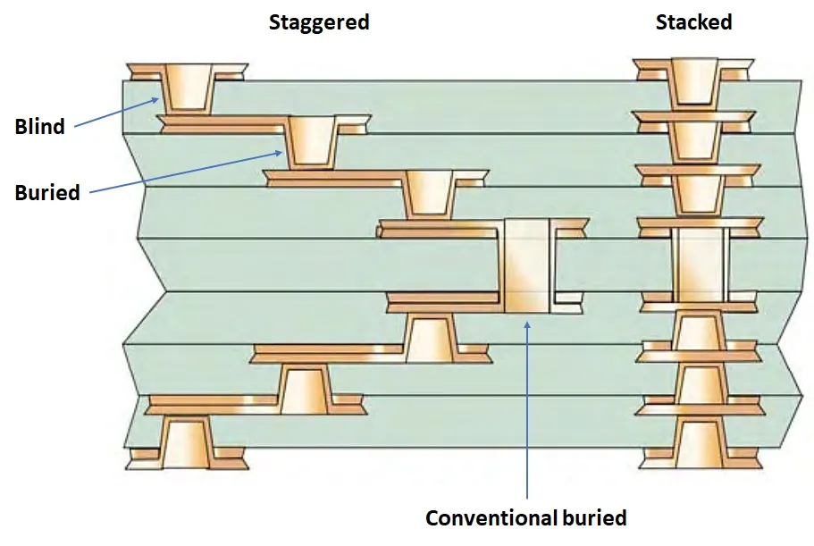
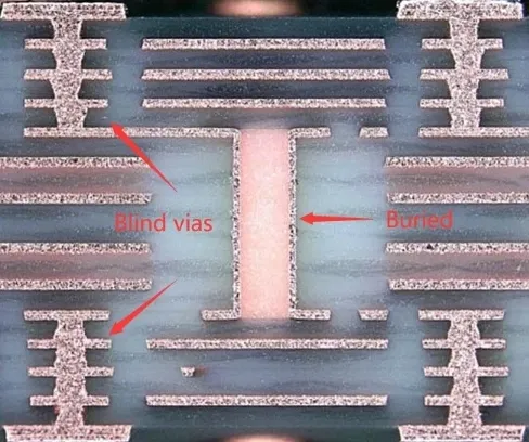
- Blind Microvias: Connect the outer layer to an inner layer but don’t go through the entire board.
- Buried Microvias: Connect inner layers only, hidden within the board structure.
- Stacked Microvias: Multiple microvias aligned on top of each other for complex multilayer designs.
Buried Vias in Rigid PCB: What You Need to Know
Buried vias are connections that link internal layers of a PCB without reaching the outer surfaces. In a buried via rigid PCB, these vias are completely hidden inside the board, making them invisible from the top or bottom. This technique is often used in HDI designs to free up space on the outer layers for more components or traces.
Unlike through-hole vias, which pass through the entire board, buried vias connect only specific inner layers. For example, in a 10-layer PCB, a buried via might connect layers 3 to 5, leaving layers 1, 2, and 6-10 untouched. This targeted connection reduces clutter on the surface and allows for denser routing.
Buried vias are especially useful in advanced rigid PCB design for applications like automotive electronics, where reliability and space efficiency are critical. They help reduce electromagnetic interference (EMI) by keeping high-speed signals contained within inner layers. However, manufacturing buried vias adds complexity and cost, as it requires sequential lamination processes to build the board layer by layer.
Advantages of Buried Via Rigid PCB
- Space Efficiency: Frees up outer layers for additional components or routing.
- Signal Protection: Shields sensitive signals from external interference.
- Improved Density: Supports more connections in multilayer boards.
Why Use Advanced Rigid PCB Design Techniques?
Advanced rigid PCB design, incorporating HDI, microvias, and buried vias, offers significant advantages over traditional methods. These techniques are essential for meeting the demands of modern electronics, where size, speed, and reliability are non-negotiable. Here are some reasons why engineers turn to these methods:
- Miniaturization: Devices like wearables and IoT gadgets require tiny boards with high functionality. HDI rigid PCBs make this possible by shrinking the footprint without sacrificing performance.
- High-Speed Performance: Microvias and buried vias shorten signal paths, reducing latency and supporting data rates above 10 Gbps, which is vital for 5G and high-speed computing.
- Reliability: Advanced designs improve thermal dissipation and reduce EMI, ensuring stable operation in harsh environments like automotive or aerospace systems.
Consider a medical device like a portable ultrasound machine. Its PCB must handle high-frequency signals (up to 20 MHz) while fitting into a handheld unit. An HDI rigid PCB with microvias and buried vias allows for a compact layout, maintains signal clarity, and ensures the device operates reliably during critical use.
Challenges in Advanced Rigid PCB Design
While the benefits are clear, advanced rigid PCB design comes with challenges. Understanding these hurdles can help engineers plan better and avoid costly mistakes.
- Manufacturing Complexity: Techniques like microvias and buried vias require precise laser drilling and sequential lamination, increasing production time and cost.
- Design Constraints: Narrow traces and tight spacing demand strict adherence to design rules. A single error in trace width (e.g., deviating from 3 mils to 2.5 mils) can lead to signal issues or manufacturing defects.
- Thermal Management: High-density designs generate more heat. Without proper planning, components can overheat, reducing lifespan. For example, a board with a power density of 5 W per square inch needs careful heat dissipation strategies.
To overcome these challenges, engineers must work closely with fabrication teams to ensure designs are manufacturable. Using simulation tools to test signal integrity and thermal performance before production can also prevent issues down the line.
How to Implement HDI, Microvias, and Buried Vias in Your Design
If you're ready to incorporate these advanced techniques into your next project, follow these practical steps to ensure success in advanced rigid PCB design:
- Define Requirements: Determine the layer count, signal speed, and space constraints. For instance, a design for a 5G module might need 10 layers and support for 28 GHz signals.
- Choose the Right Vias: Use microvias for surface-to-inner layer connections and buried vias for internal links to optimize space. Ensure via sizes match your design needs, such as 4 mils for microvias in dense areas.
- Plan Trace Routing: Keep traces short and direct, especially for high-speed signals. Maintain impedance control, targeting values like 50 ohms for single-ended signals or 100 ohms for differential pairs.
- Collaborate with Manufacturers: Share your design early to confirm capabilities for HDI processes, microvia drilling, and buried via lamination. Verify minimum tolerances, such as 3-mil trace widths.
- Test and Validate: Use simulation software to check signal integrity and thermal performance. Build prototypes to test real-world behavior before full production.
By following these steps, you can leverage HDI rigid PCB, microvia rigid PCB, and buried via rigid PCB techniques to create cutting-edge designs that meet modern demands.
Applications of Advanced Rigid PCB Techniques
These advanced methods are used across various industries, driving innovation in electronics. Here are some key applications:
- Consumer Electronics: Smartphones and tablets rely on HDI rigid PCBs for compact, high-performance designs. Microvias enable dense BGA layouts for processors and memory chips.
- Automotive Systems: Advanced driver-assistance systems (ADAS) use buried via rigid PCBs to handle high-speed data and ensure reliability in harsh conditions.
- Medical Devices: Portable diagnostics and implantable devices benefit from miniaturization through HDI and microvia technology, ensuring precision and patient safety.
- Aerospace and Defense: High-reliability boards with buried vias protect critical signals from interference, supporting mission-critical systems.
Conclusion: Mastering Advanced Rigid PCB Design
Advanced rigid PCB techniques like HDI, microvias, and buried vias are transforming the way we design electronics. By adopting HDI rigid PCB technology, you can achieve higher component density and better performance in smaller spaces. Microvia rigid PCB designs enable precise connections for high-speed signals, while buried via rigid PCB structures optimize space and protect sensitive signals. Together, these methods empower engineers to tackle the challenges of modern electronics with confidence.
At ALLPCB, we’re committed to helping you bring your advanced rigid PCB designs to life. Whether you're working on consumer gadgets or industrial systems, understanding and applying these techniques will give you a competitive edge. Keep exploring, testing, and refining your designs to stay ahead in this fast-evolving field.


