 ALLPCB


In the fast-evolving world of smart home technology, creating innovative and reliable devices starts with effective PCB prototyping. Whether you're designing a smart thermostat, a connected lighting system, or a home security sensor, the right PCB prototyping techniques can make or break your project. This blog explores advanced methods like rapid PCB prototyping, PCB milling, 3D printing for PCBs, and online PCB prototyping services, helping you bring your smart home ideas to life faster and more efficiently.
At ALLPCB, we understand the unique challenges faced by engineers and innovators in the smart home sector. That’s why we’ve compiled this detailed guide to help you navigate the latest prototyping methods, ensuring your designs are both cutting-edge and practical. Let’s dive into the world of PCB prototyping and discover how these techniques can accelerate your smart home innovations.
Why PCB Prototyping is Crucial for Smart Home Innovations
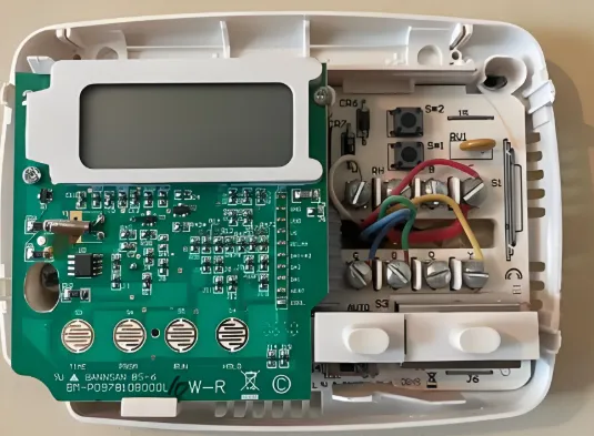
Smart home devices rely on compact, efficient, and highly functional printed circuit boards (PCBs) to operate seamlessly. These devices often integrate sensors, microcontrollers, and wireless communication modules, requiring precise PCB designs to handle low-power consumption and high-speed signals. For instance, a smart doorbell may need to process video data at speeds exceeding 100 Mbps while maintaining signal integrity with impedance values around 50 ohms for optimal performance.
Prototyping allows engineers to test and refine these designs before mass production, minimizing costly errors. With the smart home market growing rapidly, shaving days or weeks off the development cycle through advanced prototyping methods can give you a competitive edge. Let’s explore some of the most effective PCB prototyping techniques for smart home innovations.
Key PCB Prototyping Techniques for Smart Home Projects
Modern PCB prototyping methods have evolved to meet the demands of complex smart home systems. Below, we’ll break down the most advanced techniques, focusing on their benefits, applications, and how they can streamline your development process.
1. Rapid PCB Prototyping: Speeding Up Development
Rapid PCB prototyping is a game-changer for smart home innovators who need to iterate designs quickly. This method focuses on producing functional prototypes in as little as 24 to 48 hours, allowing engineers to test concepts and make adjustments without long delays. For example, if you’re designing a smart light switch with Wi-Fi connectivity, rapid prototyping lets you test signal integrity and power consumption early, ensuring the board supports frequencies around 2.4 GHz without interference.
The process often involves automated design tools and fast fabrication services, reducing turnaround time significantly. This is especially useful for smart home devices where market trends shift quickly, and being first to market can define success. By leveraging rapid PCB prototyping, you can validate your designs faster and move closer to production readiness.
2. PCB Milling: Precision for Custom Designs
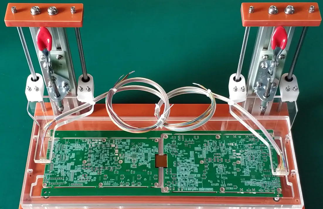
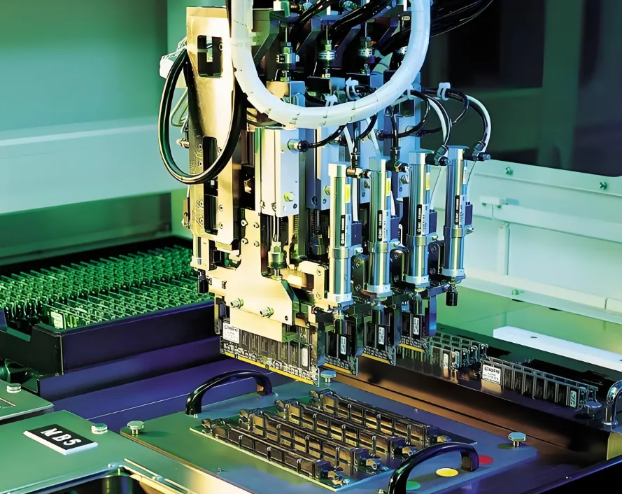
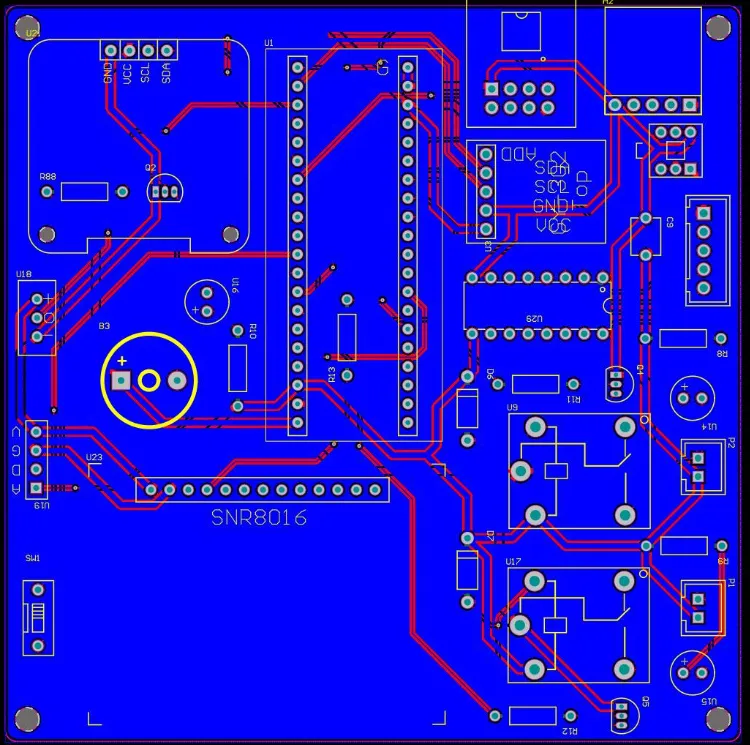
PCB milling is a subtractive manufacturing technique that uses a CNC machine to carve out copper traces from a blank board. This method is ideal for creating small batches of prototypes with high precision, especially for smart home devices that require custom layouts. For instance, a smart sensor for humidity monitoring might need a unique board shape to fit into a compact enclosure, and milling offers the flexibility to achieve this without expensive tooling.
One major advantage of PCB milling is the ability to produce prototypes in-house, cutting down on shipping times and costs. Modern milling machines can achieve trace widths as small as 0.1 mm, ensuring even complex smart home circuits with dense component placement are feasible. Additionally, milling avoids the use of harsh chemicals found in traditional etching processes, making it a more environmentally friendly option for prototyping.
However, PCB milling is best suited for low-volume runs or initial designs, as it can be slower and less cost-effective for larger quantities compared to other methods. Still, for engineers working on bespoke smart home solutions, it remains a powerful tool in the prototyping arsenal.
3. 3D Printing PCB: Innovating with Additive Manufacturing
3D printing for PCBs, also known as additive manufacturing, is an emerging technique that’s revolutionizing how prototypes are made. Unlike traditional methods, 3D printing builds the board layer by layer, often integrating conductive materials like silver ink for traces alongside insulating substrates. This approach is particularly exciting for smart home innovations, where unconventional board shapes or integrated components can enhance device functionality.
For example, imagine a smart wearable device for home automation control that wraps around a user’s wrist. 3D printing allows you to create a flexible or curved PCB that fits perfectly within the device’s design, something traditional rigid boards can’t achieve. Some advanced 3D printers can even embed components like resistors or capacitors directly into the board during printing, reducing assembly time.
While 3D printing PCB technology is still developing and may not yet match the precision of milled or etched boards for high-frequency applications (like those above 5 GHz), it offers unparalleled design freedom. It’s an excellent choice for early-stage prototypes or proof-of-concept designs in the smart home space.
4. Online PCB Prototyping Services: Convenience and Scalability
For engineers who prefer to outsource fabrication, online PCB prototyping services provide a hassle-free way to turn designs into reality. These platforms allow you to upload your design files, specify requirements like layer count or material type, and receive finished prototypes within days. This method is ideal for smart home projects that require quick validation without investing in in-house equipment.
Many online services cater to the specific needs of smart home innovators, offering options like high-density interconnect (HDI) boards for compact devices or materials with low dielectric constants for better signal performance at frequencies up to 2.4 GHz or higher. Additionally, these services often provide cost-effective solutions for small-batch runs, making them perfect for testing multiple iterations of a smart lock or thermostat design.
The key benefit of online prototyping is scalability. Once your smart home device prototype is finalized, the same service can often transition seamlessly into full-scale production, saving time and ensuring consistency. This streamlined approach helps you focus on design and functionality rather than manufacturing logistics.
Choosing the Right Prototyping Method for Your Smart Home Project
Selecting the best PCB prototyping technique depends on your project’s specific needs, timeline, and budget. Here’s a quick breakdown to help you decide:
- Rapid PCB Prototyping: Best for tight deadlines and iterative testing of smart home devices with standard designs.
- PCB Milling: Ideal for custom or small-batch prototypes where precision and in-house control are priorities.
- 3D Printing PCB: Perfect for experimental designs or non-traditional board shapes in innovative smart home products.
- Online PCB Prototyping Services: Suited for engineers seeking convenience, scalability, and professional-grade results without in-house equipment.
Consider the technical requirements of your smart home device as well. For instance, if your design involves high-speed communication protocols like Zigbee or Bluetooth with impedance control around 50 ohms, rapid prototyping or online services might offer the best accuracy. On the other hand, for a unique form factor in a wearable smart home controller, 3D printing could be the way to go.
Benefits of Advanced Prototyping for Smart Home Innovations
Adopting these advanced PCB prototyping methods offers several advantages for smart home development:
- Faster Time-to-Market: Techniques like rapid prototyping and online services cut down development cycles, helping you launch products sooner.
- Cost Efficiency: By identifying design flaws early through prototypes, you avoid expensive revisions during production.
- Innovation Enablement: Methods like 3D printing allow for creative designs that push the boundaries of traditional smart home devices.
- Improved Reliability: Testing prototypes under real-world conditions ensures your smart home products meet performance and safety standards.
For example, a smart energy monitor might require multiple prototype iterations to optimize power efficiency to below 1 mW in standby mode. Using rapid prototyping or online services, you can test various layouts and components swiftly, ensuring the final product is both effective and market-ready.
Tips for Effective PCB Prototyping in Smart Home Design
To maximize the value of these prototyping methods, keep the following tips in mind:
- Start with Clear Specifications: Define your smart home device’s requirements, such as power needs or signal frequencies, before prototyping to avoid wasted iterations.
- Test Under Real Conditions: Simulate the operating environment of your device during testing. For instance, test a smart thermostat PCB at varying temperatures to ensure reliability.
- Leverage Design Software: Use advanced PCB design tools to simulate performance and identify issues before physical prototyping.
- Document Iterations: Keep detailed records of each prototype version to track improvements and inform final production decisions.
Conclusion: Powering Smart Home Innovations with Advanced PCB Prototyping
The smart home industry thrives on innovation, and advanced PCB prototyping methods are at the heart of bringing new ideas to life. From rapid PCB prototyping that accelerates development to PCB milling for precise custom designs, 3D printing for groundbreaking form factors, and online PCB prototyping services for convenience, these techniques empower engineers to create reliable, cutting-edge devices.
At ALLPCB, we’re committed to supporting your smart home projects with solutions tailored to your prototyping needs. By choosing the right method for your design, you can reduce costs, speed up development, and deliver products that transform how people live. Embrace these advanced prototyping techniques and watch your smart home innovations come to life with efficiency and impact.


