 ALLPCB


In the world of high-speed electronics, a well-designed 6-layer PCB stackup is the backbone of ensuring signal integrity and performance. Whether you're working on telecommunications, computing, or advanced consumer electronics, optimizing a 6-layer PCB stackup for impedance control, crosstalk minimization, and high-speed routing can make or break your design. In this comprehensive guide, we'll uncover the secrets to crafting a 6-layer PCB stackup that supports high-speed designs while maintaining signal integrity. We'll dive into topics like impedance control, material selection, routing guidelines, simulation techniques, and crosstalk minimization—all tailored for engineers seeking practical solutions.
Let’s explore how to build a robust 6-layer PCB stackup that meets the demands of modern high-speed applications, ensuring your designs perform reliably under challenging conditions.
Why a 6-Layer PCB Stackup Matters for High-Speed Designs
A 6-layer PCB stackup offers a balance between complexity and cost, making it a popular choice for designs requiring multiple signal layers, power distribution, and ground planes. Unlike simpler 2- or 4-layer boards, a 6-layer configuration provides enough room to separate high-speed signals, reduce electromagnetic interference (EMI), and maintain controlled impedance. This is critical for applications like USB 3.0, HDMI, or DDR memory interfaces, where signal speeds often exceed 1 GHz.
The primary goal of a 6-layer stackup is to ensure signal integrity, which refers to the ability of a signal to travel from source to destination without distortion, loss, or interference. Poor stackup design can lead to issues like crosstalk, signal reflections, or EMI, all of which degrade performance. By carefully planning the arrangement of signal, power, and ground layers, you can minimize these risks and achieve a stable, high-performing design.
Designing a 6-Layer PCB Stackup for Impedance Control
Impedance control is a cornerstone of high-speed design, especially in a 6-layer PCB where signal traces often run close to each other. Controlled impedance ensures that signals travel without reflections, which can occur when there’s a mismatch between the trace impedance and the connected components. For high-speed signals, a common target impedance is 50 ohms for single-ended traces or 100 ohms for differential pairs.
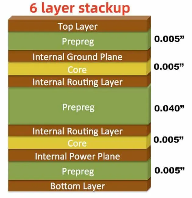
To achieve 6-layer PCB stackup impedance control, start by defining the layer arrangement. A typical 6-layer stackup might look like this:
- Layer 1: Top signal layer for high-speed traces
- Layer 2: Ground plane
- Layer 3: Power plane
- Layer 4: Power plane or additional ground
- Layer 5: Ground plane
- Layer 6: Bottom signal layer
This configuration places ground planes near signal layers to provide a consistent reference for impedance and reduce EMI. The distance between a signal layer and its adjacent ground plane, along with the dielectric material’s properties, determines the trace impedance. For instance, a trace width of 5 mils (0.127 mm) on a 1.6 mm thick board with a dielectric constant (Dk) of 4.2 might yield a 50-ohm impedance when spaced 0.2 mm from the ground plane. Use an impedance calculator or simulation tool to fine-tune these values based on your specific board materials and thickness.
Maintaining symmetry in the stackup is also crucial. An unbalanced stackup can cause warping during manufacturing, leading to signal integrity issues. Ensure that dielectric thicknesses are consistent between layers, and consult with your fabrication partner to verify manufacturability.
Material Selection for Signal Integrity in 6-Layer PCBs
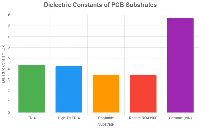
The choice of materials plays a massive role in maintaining signal integrity, especially for high-speed designs. When focusing on 6-layer PCB material selection for signal integrity, two key factors to consider are the dielectric constant (Dk) and the dissipation factor (Df) of the substrate material.
Standard FR-4 material, with a Dk of around 4.2 to 4.5, works well for many applications but may introduce signal loss at frequencies above 1 GHz due to its higher Df (around 0.02). For high-speed designs operating at 5 GHz or more, consider low-loss materials like Isola 370HR (Dk ~3.9, Df ~0.009) or Rogers RO4350B (Dk ~3.5, Df ~0.0037). These materials minimize signal attenuation and ensure better performance for high-frequency signals.
Additionally, pay attention to the copper foil type. Rough copper surfaces can increase signal loss at high frequencies due to the skin effect, where current flows near the surface of the conductor. Opt for smoother copper foils, such as rolled annealed (RA) copper, to reduce loss in critical signal paths.
The dielectric thickness between layers also impacts impedance and crosstalk. Thinner dielectrics (e.g., 0.1 mm) allow tighter coupling between signal and ground layers, improving impedance control but increasing manufacturing costs. Balance performance with budget by selecting materials and thicknesses that meet your design’s frequency and speed requirements.
High-Speed Routing Guidelines for 6-Layer PCBs
Routing high-speed signals on a 6-layer PCB requires careful planning to avoid interference and maintain signal quality. Following 6-layer PCB high-speed routing guidelines can significantly improve your design’s performance. Here are some practical tips:
- Minimize Trace Lengths: Keep high-speed signal traces as short as possible to reduce delay and signal loss. For example, in a 10 Gbps signal, a 1-inch (25.4 mm) trace can introduce noticeable propagation delay (around 150 ps).
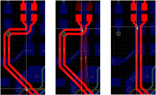
- Avoid Sharp Corners: Use 45-degree angles or curved traces instead of 90-degree bends to prevent signal reflections caused by impedance discontinuities.
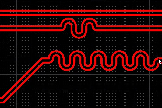
- Route Differential Pairs Together: For differential signals like USB or Ethernet, keep the pair’s traces parallel and matched in length to within 5 mils (0.127 mm) to avoid skew.
- Isolate High-Speed Signals: Place high-speed traces on outer layers near ground planes, and avoid routing them over splits in power or ground planes, as this can disrupt the return path and cause EMI.
- Use Via Stitching: Add ground vias near high-speed signal vias to provide a low-impedance return path and reduce crosstalk.
Layer assignment is also critical. Reserve the top and bottom layers for high-speed signals and sensitive analog traces, while using inner layers for power distribution or slower digital signals. This separation reduces interference and keeps critical signals close to their reference planes.
Signal Integrity Simulation for 6-Layer PCBs
Before sending your design for fabrication, performing 6-layer PCB signal integrity simulation is a must to identify potential issues like reflections, crosstalk, or timing errors. Simulation tools allow you to model your stackup, trace geometry, and material properties to predict how signals will behave in real-world conditions.
Start by simulating impedance for critical traces. Tools can calculate the characteristic impedance of a trace based on its width, thickness, and proximity to the ground plane. For instance, a simulation might reveal that a 6-mil-wide trace on a 0.2 mm dielectric achieves a 50-ohm impedance, helping you adjust dimensions if needed.
Next, run time-domain reflectometry (TDR) simulations to detect impedance mismatches along the signal path. This can highlight issues like via stubs or poorly terminated traces that cause reflections. Additionally, perform eye diagram analysis for high-speed digital signals to ensure sufficient voltage margins and timing windows at data rates like 5 Gbps or higher.
Simulations should also include power integrity analysis to verify that power delivery networks (PDNs) can handle transient currents without causing voltage drops or noise. A well-designed PDN in a 6-layer PCB typically includes multiple ground planes and decoupling capacitors placed near high-current components.
Crosstalk Minimization Techniques for 6-Layer PCBs
Crosstalk, the unwanted coupling of signals between adjacent traces, is a common challenge in high-speed designs. Implementing 6-layer PCB crosstalk minimization techniques can significantly improve signal quality. Here are proven strategies to reduce crosstalk:
- Increase Trace Spacing: Maintain a spacing of at least 3 times the trace width between adjacent high-speed traces. For a 5-mil trace, this means a 15-mil separation to minimize coupling.
- Use Ground Planes as Shields: Route high-speed signals on layers adjacent to continuous ground planes. The ground plane acts as a shield, absorbing stray electromagnetic fields.
- Route Signals on Different Layers: If spacing is limited, route aggressor and victim traces on different layers with a ground plane between them to block interference.
- Minimize Parallel Runs: Avoid long parallel runs of high-speed traces, as they increase the opportunity for crosstalk. If unavoidable, keep parallel sections under 500 mils (12.7 mm) in length.
- Add Guard Traces: Place grounded guard traces between critical signals to isolate them from each other. Connect these traces to ground at multiple points using vias.
Crosstalk is also influenced by signal rise time. Faster rise times (e.g., under 100 ps) increase the likelihood of coupling, so consider slowing down edges if performance allows. Simulation tools can help quantify crosstalk levels and guide adjustments to trace spacing or layer assignments.
Practical Tips for a Successful 6-Layer PCB Design
Beyond the technical aspects, a few practical considerations can ensure your 6-layer PCB design succeeds from concept to production:
- Collaborate Early with Fabricators: Share your stackup and material choices with your manufacturing partner to confirm they can meet tolerances for trace widths, dielectric thicknesses, and impedance control.
- Test Prototypes: Build and test prototypes to validate simulations. Use a vector network analyzer (VNA) to measure impedance and signal loss on critical paths.
- Document Design Rules: Clearly define design constraints like trace widths, spacings, and via sizes in your design software to avoid errors during layout.
- Plan for Thermal Management: High-speed designs often generate heat, so incorporate thermal vias and ensure power planes can dissipate heat effectively.
By integrating these practices into your workflow, you’ll create a 6-layer PCB that not only meets performance goals but also remains manufacturable and cost-effective.
Conclusion: Mastering 6-Layer PCB Stackup for High-Speed Success
Designing a 6-layer PCB stackup for high-speed applications is a complex but rewarding task. By focusing on impedance control, material selection, routing guidelines, signal integrity simulation, and crosstalk minimization, you can build a board that delivers exceptional performance even at multi-gigabit speeds. Each layer, trace, and material choice contributes to the overall signal quality, making attention to detail essential.
With the strategies outlined in this guide, you’re equipped to tackle the challenges of high-speed design and optimize your 6-layer PCB stackup for signal integrity. Whether you’re working on cutting-edge data systems or advanced consumer electronics, a well-planned stackup is your foundation for success. Start applying these secrets today to elevate your designs to the next level.


