ALLPCB


Designing printed circuit boards (PCBs) for 5G mobile phones comes with unique challenges due to the high-frequency signals involved. To overcome these, engineers must focus on selecting the right 5G PCB materials, optimizing high-frequency PCB layout, ensuring signal integrity in 5G systems, managing thermal issues with effective thermal management for 5G PCBs, and integrating 5G antenna PCB design. In this comprehensive guide, we’ll dive into these critical areas, offering practical solutions and insights to help engineers tackle the complexities of 5G technology.
Introduction to 5G PCB Design Challenges
The rollout of 5G technology has revolutionized mobile communication with its promise of ultra-fast speeds, low latency, and massive connectivity. However, these benefits come with significant hurdles for PCB designers. 5G operates at much higher frequencies—often in the millimeter-wave range of 24 GHz to 100 GHz—compared to 4G, which typically uses frequencies below 6 GHz. These high frequencies introduce issues like signal loss, interference, and heat buildup, demanding innovative approaches in PCB design. This blog will explore how to address these high-frequency challenges and build reliable, high-performance 5G mobile phone PCBs.
1. Choosing the Right 5G PCB Materials
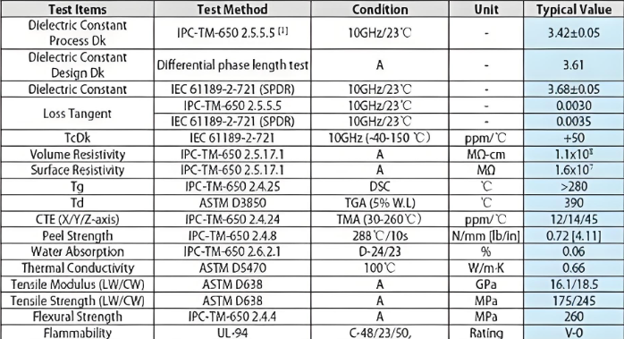
The foundation of any successful 5G PCB design lies in selecting appropriate materials that can handle high-frequency signals. At frequencies above 10 GHz, standard materials like FR-4 often fail due to high dielectric loss, which leads to signal degradation. For 5G applications, engineers need low-loss, high-performance materials with stable dielectric constants (Dk) and low dissipation factors (Df).
Common materials for 5G PCBs include polytetrafluoroethylene (PTFE)-based laminates and advanced hydrocarbon-based substrates. These materials typically have a Dk value between 2.2 and 3.5 and a Df below 0.002, minimizing signal loss at high frequencies. For example, PTFE laminates can maintain signal integrity at 28 GHz, a common 5G band, ensuring data rates remain consistent. Additionally, these materials must withstand the manufacturing process and provide mechanical stability for compact mobile phone designs.
When selecting 5G PCB materials, consider the following factors:
- Dielectric Constant (Dk): A lower and stable Dk ensures consistent signal propagation.
- Dissipation Factor (Df): A lower Df reduces energy loss, critical for millimeter-wave frequencies.
- Thermal Stability: Materials must handle heat from high-speed components without degrading.
By prioritizing these properties, designers can create PCBs that support the demanding requirements of 5G technology.
2. High-Frequency PCB Layout Techniques
The layout of a PCB plays a crucial role in managing high-frequency signals. Poor layout design can lead to signal reflection, crosstalk, and electromagnetic interference (EMI), all of which degrade 5G performance. A well-thought-out high-frequency PCB layout minimizes these risks by focusing on impedance control, trace length, and component placement.
Here are key strategies for effective high-frequency PCB layout:
- Impedance Matching: Maintain a consistent impedance, often 50 ohms for RF signals, to prevent signal reflection. Use controlled impedance traces with precise widths and spacing.
- Short Trace Lengths: Keep signal traces as short as possible to reduce loss. At 28 GHz, even a few millimeters of extra trace can cause significant attenuation.
- Ground Planes: Use continuous ground planes to provide a return path for high-frequency signals and reduce EMI. Avoid splitting ground planes under critical signal paths.
- Via Optimization: Minimize the use of vias, as they introduce inductance and capacitance. When necessary, use back-drilled or blind vias to reduce stub effects.
Additionally, separating analog and digital components on the PCB helps prevent interference. For instance, placing RF components away from noisy digital circuits ensures cleaner signal transmission. By applying these layout techniques, designers can achieve reliable performance in 5G mobile phone PCBs.
3. Ensuring Signal Integrity in 5G Systems
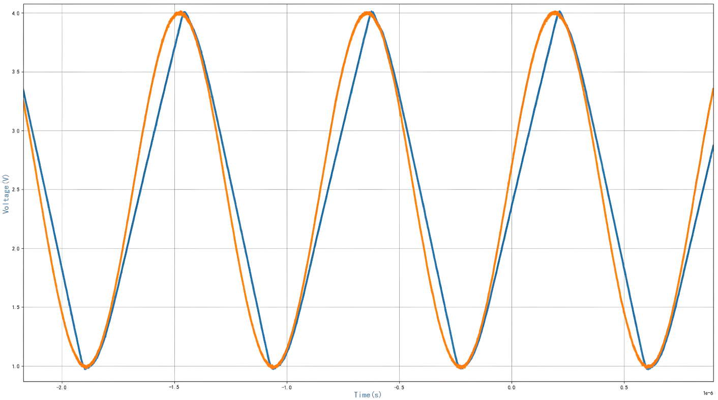
Signal integrity in 5G (SI) is paramount, as high-frequency signals are more susceptible to distortion and loss. Maintaining signal integrity ensures that data transmitted at speeds exceeding 10 Gbps remains accurate and reliable. Challenges to SI in 5G include signal attenuation, crosstalk, and timing issues caused by the skin effect and dielectric losses.
To address signal integrity in 5G, consider these practices:
- Minimize Signal Loss: Use low-loss materials and keep trace lengths short. At 28 GHz, signal loss can reach 1 dB per inch on standard materials, so advanced substrates are essential.
- Reduce Crosstalk: Space traces adequately and use shielding techniques like guard traces or grounded vias to isolate high-speed lines.
- Timing Control: Match trace lengths for differential pairs to avoid skew, ensuring synchronized data transmission.
- Simulation Tools: Employ simulation software to model signal behavior before fabrication. This helps identify potential issues like reflections or impedance mismatches early in the design process.
By focusing on these areas, engineers can maintain signal integrity in 5G systems, ensuring that mobile phones deliver the high-speed, low-latency performance users expect.
4. Thermal Management for 5G PCBs
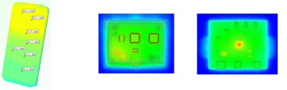
Thermal management for 5G PCBs is a critical concern due to the increased power density of components and high-frequency operation. 5G mobile phones often include multiple RF modules, high-speed processors, and power amplifiers, all generating significant heat in a compact space. Without proper thermal management, overheating can degrade performance, reduce component lifespan, and even cause device failure.
Effective thermal management strategies include:
- Heat Sinks and Thermal Vias: Integrate heat sinks for high-power components and use thermal vias to transfer heat from the top layer to a heat-dissipating layer or chassis. For example, thermal vias with a diameter of 0.3 mm can improve heat dissipation by up to 30%.
- Material Selection: Choose substrates with high thermal conductivity, such as ceramic-filled laminates, to spread heat evenly across the board.
- Component Placement: Position heat-generating components away from sensitive areas and near heat dissipation paths. Avoid clustering high-power parts in one area.
- Advanced Cooling: Incorporate vapor chambers or micro heat pipes in premium designs to manage heat in ultra-thin devices.
Proper thermal management for 5G PCBs ensures reliability and prevents thermal throttling, maintaining the high performance of 5G mobile phones even under heavy use.
5. 5G Antenna PCB Design Considerations
Antenna design is at the heart of 5G mobile phone performance, as it directly impacts signal reception and transmission. Unlike 4G, 5G often relies on phased array antennas and beamforming technology to focus signals in specific directions, improving efficiency and range. Integrating 5G antenna PCB design into compact devices poses unique challenges due to space constraints and high-frequency requirements.
Key considerations for 5G antenna PCB design include:
- Phased Array Integration: Phased array antennas consist of multiple small elements that work together to steer signals. These require precise placement and routing on the PCB to maintain phase alignment, often within 0.1 mm accuracy.
- Material Compatibility: Use low-loss materials to prevent signal attenuation at the antenna interface. A dissipation factor below 0.001 is ideal for millimeter-wave antennas.
- Compact Design: Antennas must fit within the limited space of a mobile phone. Techniques like antenna-in-package (AiP) integrate the antenna directly into the chip package, saving space on the PCB.
- Interference Mitigation: Shield antennas from nearby components to avoid EMI. Use metal enclosures or grounded layers to isolate the antenna area.
By optimizing 5G antenna PCB design, engineers can ensure robust connectivity and support advanced features like beamforming, which are essential for 5G performance.
Conclusion: Building the Future of 5G with Advanced PCB Design
Designing PCBs for 5G mobile phones is no small feat. The high-frequency challenges of signal loss, interference, heat buildup, and compact antenna integration demand careful planning and innovative solutions. By focusing on the right 5G PCB materials, implementing high-frequency PCB layout best practices, ensuring signal integrity in 5G systems, prioritizing thermal management for 5G PCBs, and optimizing 5G antenna PCB design, engineers can create devices that deliver on the promise of 5G technology.
At ALLPCB, we’re committed to supporting designers with the tools and expertise needed to overcome these challenges. Whether it’s selecting advanced materials or refining layouts for high-frequency performance, our goal is to help bring cutting-edge 5G solutions to life. With the right approach, the future of mobile connectivity is within reach.
Suggested Image Placement: Place a final image here showing a completed 5G mobile phone PCB with key components highlighted. ALT Text: "Completed 5G mobile phone PCB design with highlighted components."