 ALLPCB


If you're an electrical engineer wondering why 1 oz copper PCBs remain the standard in electronics design, the answer lies in their balance of performance, cost, and versatility. With a thickness of approximately 1.37 mils (34.79 microns), 1 oz copper PCBs offer sufficient current-carrying capacity for most applications while being cost-effective and easy to manufacture. In this blog, we'll dive deep into the advantages of 1 oz copper PCBs, their applications, manufacturing processes, costs, and why they continue to dominate as the standard copper thickness for printed circuit boards.
What Is a 1 oz Copper PCB?
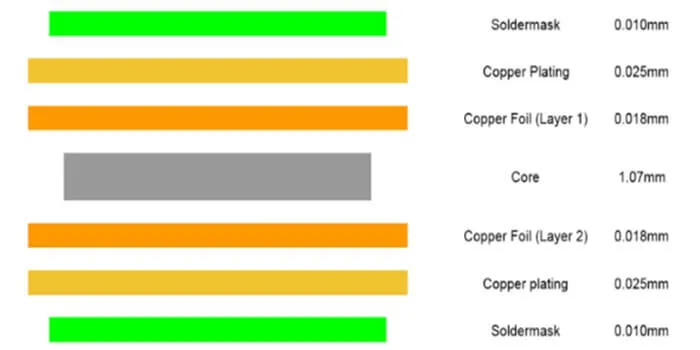
A 1 oz copper PCB refers to a printed circuit board where the copper layer weighs 1 ounce per square foot. This translates to a thickness of about 1.37 mils or 34.79 microns. This weight and thickness are considered the industry standard for most PCB designs because they provide a good balance between electrical performance and manufacturability. The copper is evenly spread across the board, ensuring consistent conductivity and thermal management for a wide range of electronic devices.
For engineers, understanding copper thickness is critical because it directly impacts a PCB's ability to handle current, manage heat, and maintain signal integrity. While thicker copper (like 2 oz or 4 oz) is used for high-power applications, and thinner copper (like 0.5 oz) for fine-line circuits, 1 oz copper strikes a middle ground that suits most general-purpose electronics.
Advantages of 1 oz Copper PCB
The widespread use of 1 oz copper PCBs in electronics isn't by chance. They offer several key benefits that make them the preferred choice for many engineers. Let's break down these advantages in detail:
1. Optimal Current-Carrying Capacity
For most standard electronics, 1 oz copper provides enough current-carrying capacity without the need for thicker layers. According to general PCB design guidelines, 1 oz copper can handle currents up to 4-5 amps per trace at a width of 100 mils (0.1 inches) with a temperature rise of 10°C. This makes it suitable for a wide range of consumer electronics, from smartphones to LED lighting systems, where high currents aren't typically a concern.
2. Cost-Effectiveness
One of the biggest advantages of 1 oz copper PCBs is their cost. Since this thickness is the industry standard, manufacturers have optimized their processes to produce these boards at scale, reducing production costs. For engineers working on budget-conscious projects, choosing 1 oz copper avoids the added expense of thicker copper layers, which can increase material and processing costs by 20-50% depending on the design.
3. Ease of Manufacturing
Manufacturing processes for 1 oz copper PCBs are well-established. Most PCB fabrication houses start with pre-clad laminates that have 0.5 oz copper on each side, building up to 1 oz after plating. This standard process minimizes errors during etching and ensures high yields, which translates to faster turnaround times for engineers needing prototypes or production runs.
4. Thermal Management
While not as effective as thicker copper for heat dissipation, 1 oz copper still offers decent thermal performance for low-to-medium power applications. It can maintain stable operation at temperatures up to 130°C with proper design, such as wider traces or thermal vias, making it reliable for most consumer-grade electronics.
5. Versatility Across Applications
The balanced properties of 1 oz copper make it adaptable to a variety of designs. Whether you're designing a single-layer board for a simple circuit or a multi-layer PCB for a complex device, 1 oz copper provides the flexibility to meet impedance requirements and signal integrity needs without over-engineering the board.
1 oz Copper PCB Applications
The versatility of 1 oz copper PCBs makes them a staple in many industries. Here are some common applications where this standard copper thickness shines:
1. Consumer Electronics
Devices like smartphones, tablets, and laptops often use 1 oz copper PCBs for their internal circuits. These boards handle the moderate current demands of processors, memory, and sensors while keeping costs low for mass production. For example, a typical smartphone PCB might use 1 oz copper for power distribution and signal routing across 4-6 layers.
2. LED Lighting
LED drivers and control circuits frequently rely on 1 oz copper PCBs. These boards manage currents of 1-3 amps for LED arrays, providing reliable performance without the need for thicker copper, which would increase costs unnecessarily in low-power lighting designs.
3. IoT Devices
Internet of Things (IoT) devices, such as smart sensors and home automation modules, benefit from the lightweight and cost-effective nature of 1 oz copper PCBs. These devices often operate on low power (under 1 amp), making 1 oz copper an ideal match for their compact designs.
4. Prototyping and Testing
For engineers developing prototypes, 1 oz copper PCBs are the go-to choice due to their availability and low cost. Whether you're testing a new microcontroller circuit or designing a custom sensor module, starting with 1 oz copper ensures you can iterate designs quickly without breaking the budget.
5. Automotive Electronics
In automotive applications, 1 oz copper PCBs are used for non-critical systems like infotainment and interior lighting controls. While high-power systems (like motor controllers) may require 2 oz or thicker copper, 1 oz works well for signal processing and low-power modules in vehicles.
Cost of 1 oz Copper PCB
Understanding the cost of 1 oz copper PCBs is essential for engineers managing project budgets. Several factors influence the price, but since 1 oz is the standard copper thickness, it remains one of the most economical options.
Base Cost Factors
The cost of a 1 oz copper PCB typically starts at $0.50 to $2 per square inch for small orders, depending on the manufacturer, board size, and layer count. For larger production runs (1,000+ units), prices can drop to $0.10-$0.30 per square inch due to economies of scale. These figures assume a standard 2-layer board with no special requirements like controlled impedance or high-density interconnects (HDI).
Comparison with Other Thicknesses
Compared to thicker copper options, 1 oz is significantly cheaper. A 2 oz copper PCB can cost 20-30% more due to additional material and processing time, while 3-4 oz copper might increase costs by 50% or more. On the other hand, 0.5 oz copper may save 10-15% on material costs but is less common and can increase manufacturing complexity for certain designs, offsetting the savings.
Additional Cost Considerations
Other factors affecting the cost include surface finish (e.g., HASL vs. ENIG), solder mask type, and shipping fees. For engineers, it’s worth noting that sticking with 1 oz copper often avoids extra charges for custom copper weights, as most fabricators stock this thickness as standard.
Suggested Image Placement: Include a cost comparison table or graph here for 1 oz, 2 oz, and 0.5 oz copper PCBs. ALT Text: "Cost comparison of 1 oz copper PCB vs other thicknesses."
Standard Copper Thickness PCB: Why 1 oz Reigns Supreme
In the world of PCB design, 1 oz copper is widely recognized as the standard copper thickness. But why has it earned this status? The answer lies in its history and practicality.
Historically, 1 oz copper became the default thickness during the early days of PCB manufacturing because it offered a practical balance for the technology of the time. Early electronics didn’t require high current capacities, and manufacturing processes were optimized for this weight. Over decades, as PCB technology evolved, 1 oz copper remained the baseline because it meets the needs of most applications without requiring specialized equipment or materials.
For electrical engineers, this means that 1 oz copper is supported by a vast ecosystem of design tools, manufacturing standards, and supplier networks. Most EDA (Electronic Design Automation) software defaults to 1 oz copper in trace width calculators, and fabricators keep large stocks of 1 oz pre-clad laminates, ensuring quick production times.
While thicker copper (2 oz, 4 oz) is necessary for high-power designs like electric vehicle chargers, and thinner copper (0.5 oz) for high-density circuits in wearables, 1 oz covers the vast middle ground. It’s the “just right” choice for 80-90% of PCB designs, from industrial controls to consumer gadgets.
1 oz Copper PCB Manufacturing: What Engineers Need to Know
The manufacturing process for 1 oz copper PCBs is a well-oiled machine, which is another reason for their popularity. Here’s a simplified overview of how these boards are made and key considerations for engineers during design:
Manufacturing Process
1. Starting Material: Most manufacturers begin with a laminate pre-clad with 0.5 oz copper on each side. After plating processes, this builds up to a finished thickness of 1 oz per square foot.
2. Imaging and Etching: A photoresist layer is applied, and the PCB design is transferred onto the board using UV light and a film mask. Unwanted copper is then etched away in a chemical bath, leaving only the desired traces and pads.
3. Plating: Additional copper is plated onto the traces to achieve the final 1 oz thickness. This step also reinforces vias and through-holes for multi-layer boards.
4. Finishing: The board undergoes solder mask application, surface finishing (like HASL or ENIG), and testing for defects before being cut to size.
Design Tips for 1 oz Copper PCBs
For engineers, designing with 1 oz copper requires attention to trace width and spacing to avoid issues like overheating or signal loss. Here are some practical tips:
- Trace Width: Use a trace width of at least 6-8 mils for signals and 20-50 mils for power traces carrying 1-2 amps to prevent excessive heat buildup.
- Spacing: Maintain a minimum spacing of 6 mils between traces to avoid crosstalk and ensure manufacturability at most fabs.
- Thermal Vias: Add thermal vias under heat-generating components to improve heat dissipation, as 1 oz copper has limited thermal conductivity compared to thicker options.
- Impedance Control: For high-speed designs, calculate trace widths to match impedance requirements (e.g., 50 ohms for RF signals) using tools like Saturn PCB Toolkit.
Suggested Image Placement: Place a flowchart or diagram here illustrating the 1 oz copper PCB manufacturing process. ALT Text: "Manufacturing process flowchart for 1 oz copper PCB."
Challenges and Limitations of 1 oz Copper PCBs
While 1 oz copper is ideal for many applications, it’s not without limitations. Engineers should be aware of these challenges when deciding whether to use this standard thickness:
- Limited Current Capacity: For high-power applications like motor controllers or power supplies handling over 5 amps, 1 oz copper may overheat, requiring wider traces or thicker copper (2 oz or more).
- Thermal Constraints: High-power components can generate heat that 1 oz copper struggles to dissipate, potentially leading to reliability issues without additional cooling solutions.
- Signal Integrity at High Frequencies: In very high-speed designs (above 1 GHz), 1 oz copper may introduce losses or impedance mismatches if not carefully designed, though this is often manageable with proper layout techniques.
For projects where these limitations are a concern, engineers might consider stepping up to 2 oz copper or using hybrid designs with mixed copper thicknesses on different layers.
Conclusion: Why 1 oz Copper PCBs Remain the Top Choice
For electrical engineers, 1 oz copper PCBs continue to be the go-to choice due to their proven balance of performance, cost, and manufacturability. They handle the needs of most electronics—from consumer gadgets to industrial controls—while keeping production costs low and design cycles short. With a thickness of 1.37 mils (34.79 microns), 1 oz copper offers sufficient current capacity (up to 4-5 amps per trace at 100 mils width), decent thermal management, and compatibility with standard manufacturing processes.
Whether you're prototyping a new IoT device, designing an LED driver, or building a multi-layer board for automotive electronics, 1 oz copper PCBs provide the reliability and flexibility you need. While they may not suit every high-power or high-frequency application, their advantages in cost and versatility make them the default standard copper thickness for PCB design.


