 ALLPCB


If you're diving into double-sided PCB design, understanding the different types of vias is crucial for creating efficient, reliable, and high-performing circuit boards. Vias are small pathways that connect the layers of a PCB, allowing signals and power to travel between the top and bottom sides. In this comprehensive guide, we’ll explore the essentials of double-sided PCB via design, including through-hole vias, blind vias, buried vias, and via stitching. Whether you're a beginner or an experienced engineer, this post will help you choose the right via type for your project and optimize your PCB layout for performance and manufacturability.
Let’s break down each via type, their applications, design considerations, and best practices to ensure your double-sided PCB design stands out in terms of functionality and reliability.
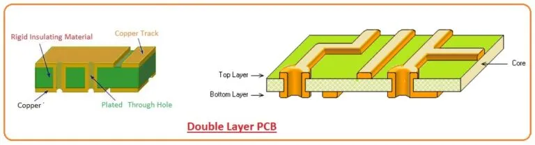
What Are Vias in Double-Sided PCB Design?
In double-sided PCB via design, vias are conductive holes or pathways that connect the copper layers on the top and bottom of the board. Unlike single-sided PCBs, which only have conductive traces on one side, double-sided PCBs utilize both sides for routing, making vias essential for electrical connections between layers. These connections are vital for routing complex circuits in a compact space, improving signal integrity, and managing power distribution.
Vias come in various types, each serving a specific purpose depending on the design requirements. Choosing the right via type can impact the board’s performance, manufacturing cost, and overall reliability. Let’s dive into the most common via types used in double-sided PCB design and explore their unique characteristics.
Why Vias Matter in Double-Sided PCB Design
Double-sided PCBs offer more space for components and traces compared to single-sided boards, but they also introduce complexity in routing. Vias help manage this complexity by enabling connections between layers without cluttering the board. Properly designed vias reduce signal loss, minimize electromagnetic interference (EMI), and ensure efficient power delivery. For high-frequency designs, vias also play a role in controlling impedance, which can affect signal speeds—often measured in gigahertz (GHz) for modern applications like 5G or high-speed data transfer.
Types of Vias in Double-Sided PCB Design
Understanding the different via types is the foundation of effective double-sided PCB via design. Below, we’ll cover the main types—through-hole vias, blind vias, buried vias, and via stitching—along with their applications and design tips.
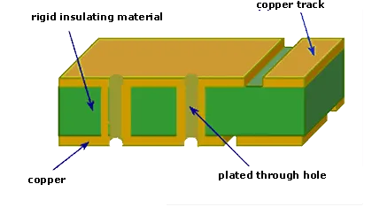
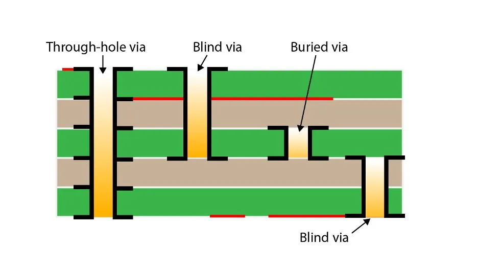
1. Through-Hole Via: The Standard Choice for Double-Sided PCBs
A through-hole via is the most common and straightforward via type used in double-sided PCB via design. These vias extend through the entire thickness of the PCB, connecting the top and bottom layers directly. They are drilled from one side of the board to the other and then plated with a conductive material, usually copper, to create an electrical pathway.
Key Features of Through-Hole Vias
- Size: Typically larger than other via types, with diameters ranging from 0.2 mm to 1 mm, depending on the design and current requirements.
- Cost: Cost-effective and easy to manufacture, making them ideal for simpler designs.
- Applications: Used in power connections, ground planes, and low-frequency signal routing.
Advantages of Through-Hole Vias
Through-hole vias are robust and reliable, capable of handling higher current loads—often up to 2-3 amps per via, depending on the copper thickness (usually 1-2 oz per square foot). They are also easier to inspect and repair, which is beneficial for prototyping and testing phases.
Design Considerations for Through-Hole Vias
When incorporating through-hole vias in your double-sided PCB, ensure proper spacing to avoid signal interference. A general rule is to maintain a clearance of at least 0.2 mm between vias and adjacent traces to prevent short circuits. Additionally, consider the aspect ratio (depth-to-diameter ratio) during manufacturing—most fabricators recommend keeping this ratio below 10:1 to ensure reliable plating.
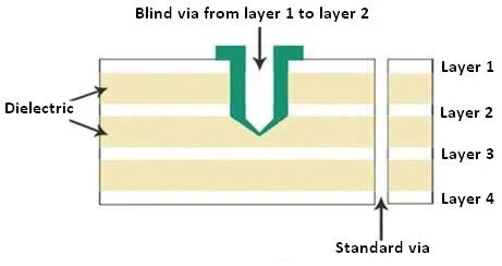
2. Blind Via in Double-Sided PCB: Space-Saving Solution
A blind via double-sided PCB design uses vias that connect an outer layer (top or bottom) to an inner layer but do not pass through the entire board. In the context of double-sided PCBs, blind vias are less common since these boards typically have only two layers. However, they can be relevant when considering future scalability to multilayer designs or when working with specific manufacturing techniques.
Key Features of Blind Vias
- Depth: Only extends partially through the board, typically connecting the surface to an internal plane.
- Size: Smaller than through-hole vias, often with diameters of 0.1-0.15 mm.
- Cost: More expensive to manufacture due to precise drilling and plating processes.
Advantages of Blind Vias
Blind vias save space on the opposite side of the board since they don’t occupy surface area on both layers. This can be useful for dense designs where component placement is critical. They also help reduce signal stub effects in high-speed designs, improving signal integrity at frequencies above 1 GHz.
Design Considerations for Blind Vias
In blind via double-sided PCB designs, ensure your manufacturer supports this technology, as it requires advanced drilling techniques like laser drilling. Additionally, blind vias have lower current-carrying capacity compared to through-hole vias, so they are better suited for signal routing rather than power delivery.
3. Buried Via in Double-Sided PCB: Hidden Connections
Similar to blind vias, buried vias are not typically used in standard double-sided PCBs because they connect internal layers without reaching the surface. In buried via double-sided PCB designs, they are rare since double-sided boards lack internal layers. However, they are worth mentioning for engineers considering hybrid or multilayer designs as an extension of double-sided layouts.
Key Features of Buried Vias
- Location: Fully enclosed within the PCB, not visible on the surface.
- Size: Very small, often 0.1 mm or less in diameter.
- Cost: High due to complex manufacturing processes.
Advantages of Buried Vias
Buried vias maximize surface space since they don’t appear on either side of the board. They are ideal for high-density interconnects (HDI) and can help reduce EMI in high-frequency applications by minimizing exposed conductive paths.
Design Considerations for Buried Vias
For buried via double-sided PCB applications, consult with your manufacturer early in the design phase, as buried vias require specialized equipment and sequential lamination processes. They are also harder to test and repair, so thorough simulation and validation are essential before production.
4. Via Stitching in Double-Sided PCB: Enhancing Ground and Power Planes
Via stitching double-sided PCB design refers to the practice of placing multiple vias in a grid or pattern to connect ground or power planes between the top and bottom layers. This technique is often used to improve electrical performance and reduce noise in the circuit.
Key Features of Via Stitching
- Pattern: Vias are placed in a uniform grid, often spaced 0.5-1 mm apart.
- Purpose: Primarily used to connect ground planes for better EMI shielding and signal return paths.
- Type: Typically uses through-hole vias for simplicity and cost-effectiveness.
Advantages of Via Stitching
Via stitching significantly reduces ground bounce and EMI, especially in high-speed designs operating at frequencies above 500 MHz. It also improves thermal dissipation by creating additional pathways for heat to escape, which is critical for power-intensive applications drawing currents of 5 amps or more.
Design Considerations for Via Stitching
In via stitching double-sided PCB designs, avoid overusing vias, as too many can weaken the board’s structural integrity or increase manufacturing costs. A common guideline is to space vias at a distance equal to one-eighth of the wavelength of the highest frequency signal to ensure effective EMI suppression. For a 2 GHz signal, this translates to a spacing of approximately 18.75 mm, though tighter grids are often used for added safety.
Choosing the Right Via Type for Your Double-Sided PCB Design
Selecting the appropriate via type for your double-sided PCB via design depends on several factors, including the complexity of your circuit, signal speed, power requirements, and budget. Here’s a quick comparison to guide your decision:
- Through-Hole Vias: Best for general-purpose designs, power connections, and low-cost manufacturing. Ideal for currents up to 3 amps and frequencies below 500 MHz.
- Blind Vias: Useful for space-constrained designs and high-speed signals above 1 GHz, though less common in pure double-sided boards.
- Buried Vias: Rare in double-sided PCBs but relevant for HDI or hybrid designs requiring internal connections.
- Via Stitching: Essential for EMI reduction and ground plane stability in high-frequency or power-intensive applications.
Always consider the manufacturing capabilities of your chosen fabricator, as advanced via types like blind and buried vias require specialized equipment and can increase lead times and costs by 20-30% compared to standard through-hole vias.
Best Practices for Double-Sided PCB Via Design
To ensure your double-sided PCB via design performs optimally, follow these practical tips:
- Minimize Via Count: Use only as many vias as necessary to reduce manufacturing complexity and maintain board strength. Excessive vias can also introduce parasitic capacitance, affecting signal integrity at frequencies above 1 GHz.
- Optimize Placement: Place vias close to the components they serve to shorten trace lengths and reduce signal delay. For high-speed signals, aim for trace lengths under 10 mm between vias and components.
- Control Impedance: For high-frequency designs, match the via impedance to the trace impedance (typically 50 ohms for RF applications) by adjusting via diameter and pad size during simulation.
- Use Simulation Tools: Leverage PCB design software to simulate signal integrity and thermal performance before fabrication. This helps identify potential issues with via placement or sizing early in the process.
- Collaborate with Manufacturers: Discuss via specifications with your PCB fabricator to ensure compliance with their design rules, especially for smaller via sizes below 0.2 mm or advanced types like blind vias.
Common Challenges in Double-Sided PCB Via Design and How to Overcome Them
Designing vias for double-sided PCBs comes with its share of challenges. Here are some common issues and solutions:
- Signal Crosstalk: High-frequency signals can interfere with nearby vias. Solve this by increasing spacing between vias to at least 0.3 mm and using ground vias for shielding.
- Thermal Stress: Vias near high-power components may overheat. Distribute heat by adding thermal vias or increasing copper thickness to 2 oz per square foot.
- Manufacturing Defects: Poor plating or drilling can lead to unreliable vias. Work with a reputable manufacturer and specify a minimum annular ring width of 0.15 mm to ensure proper connections.
Conclusion: Mastering Via Types for Double-Sided PCB Success
Mastering double-sided PCB via design is a key step in creating efficient and reliable circuit boards. Whether you’re using through-hole vias for straightforward connections, exploring blind via double-sided PCB options for compact layouts, considering buried via double-sided PCB techniques for future scalability, or implementing via stitching double-sided PCB strategies for EMI control, each via type has a unique role to play. By understanding their features, advantages, and design considerations, you can make informed decisions that enhance your PCB’s performance and manufacturability.
Start by evaluating your project’s specific needs—signal speed, current load, and space constraints—and apply the best practices outlined in this guide. With careful planning and collaboration with your manufacturer, your double-sided PCB design will achieve optimal functionality and reliability for any application.


