 ALLPCB


In today’s fast-paced world of electronics, the demand for smaller, faster, and more efficient devices is higher than ever. Sequential Build-Up (SBU) PCBs are at the heart of this revolution, enabling High-Density Interconnects (HDI) that power miniaturized devices. If you’re wondering how HDI PCB sequential build-up works or how it supports cutting-edge technology, you’ve come to the right place. This blog will dive deep into the technology behind sequential build-up PCBs, explore processes like microvia formation sequential build-up and blind and buried vias sequential build-up, and highlight sequential build-up PCB applications in modern industries.
Whether you’re an engineer designing compact gadgets or a tech enthusiast curious about the latest advancements, this guide will break down complex concepts into simple, actionable insights. Let’s explore how sequential build-up PCBs are shaping the future of electronics.
What Are Sequential Build-Up PCBs and Why Do They Matter?
Sequential Build-Up PCBs are a specialized type of printed circuit board designed to achieve higher wiring density in a smaller footprint. Unlike traditional PCBs, which are built in a single process, SBU technology involves adding layers of insulation and copper sequentially. This method allows for the integration of advanced features like microvias and blind or buried vias, making it a cornerstone of HDI technology.
The primary goal of HDI PCB sequential build-up is to pack more functionality into less space. As devices like smartphones, wearables, and medical equipment continue to shrink, the need for intricate circuitry grows. SBU PCBs meet this demand by enabling finer traces (often below 75 micrometers) and smaller vias (down to 50 micrometers in diameter), which traditional manufacturing struggles to achieve.
How Does Sequential Build-Up Technology Work?
The process of creating a sequential build-up PCB is a multi-step journey that requires precision at every stage. Here’s a breakdown of how it works:
1. Core Layer Fabrication
The process begins with a core layer, typically made of a thin insulating material like FR-4 or a high-performance laminate. This core serves as the foundation for the board. Copper is laminated onto both sides of the core, forming the initial circuitry through etching.
2. Layer Addition Through Sequential Build-Up
Once the core is ready, additional layers of insulation and copper are added one at a time. Each layer is bonded to the previous one using heat and pressure. This sequential approach allows manufacturers to control the placement of vias and traces with extreme accuracy, a key factor in achieving high-density interconnects.
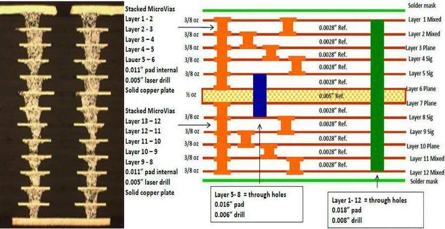
3. Microvia Formation in Sequential Build-Up
Microvia formation sequential build-up is a critical step in HDI PCB design. Microvias are tiny holes (often less than 150 micrometers in diameter) that connect different layers of the PCB. These vias are created using laser drilling, which offers precision that mechanical drilling can’t match. After drilling, the microvias are plated with copper to ensure reliable electrical connections.
4. Blind and Buried Vias in Sequential Build-Up
Another standout feature of SBU technology is the use of blind and buried vias sequential build-up. Blind vias connect an outer layer to an inner layer without passing through the entire board, while buried vias connect internal layers only. These vias save space on the PCB surface, allowing for denser layouts and improved signal integrity by reducing parasitic capacitance and inductance.
Key Benefits of Sequential Build-Up PCBs for High-Density Interconnects
Sequential build-up technology offers several advantages that make it ideal for modern electronics. Here are some of the most significant benefits:
- Space Efficiency: By using microvias and blind/buried vias, SBU PCBs reduce the need for large through-holes, freeing up space for more components. This is crucial for devices like smartwatches, where every millimeter counts.
- Enhanced Signal Performance: Shorter interconnects and finer traces (down to 3 mils or 0.076 mm) minimize signal loss and crosstalk. This results in faster data transmission, with some HDI designs supporting speeds up to 10 Gbps.
- Improved Reliability: The precise manufacturing process reduces the risk of defects, ensuring consistent performance even in harsh environments like automotive or aerospace applications.
- Flexibility in Design: SBU allows for complex stack-ups (e.g., 6+N+6 configurations, where N represents core layers) tailored to specific needs, from simple 4-layer boards to intricate 20-layer designs.
Challenges in Sequential Build-Up PCB Manufacturing
While the benefits are clear, SBU technology isn’t without its challenges. Understanding these hurdles can help engineers make informed decisions during the design phase.
- Higher Costs: The sequential addition of layers and the use of advanced techniques like laser drilling increase manufacturing costs compared to standard PCBs. For instance, adding just two build-up layers can raise costs by 20-30%.
- Complex Processes: Each build-up layer requires precise alignment and bonding, increasing production time. A single misalignment can lead to signal integrity issues or board failure.
- Material Limitations: High-frequency applications often require specialized materials like polyimide or low-loss laminates, which can handle dielectric constants as low as 2.2 but are more expensive.
Sequential Build-Up PCB Applications in Miniaturized Devices
The versatility of sequential build-up PCB applications makes them indispensable across various industries. Here are some key areas where this technology shines:
1. Consumer Electronics
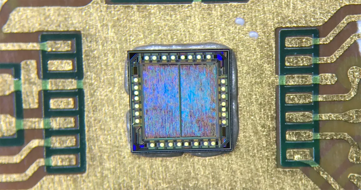
Smartphones, tablets, and wearable devices rely heavily on HDI PCBs to fit powerful hardware into compact designs. For example, modern smartphones often use 8- to 12-layer SBU PCBs with microvias as small as 60 micrometers to support high-speed processors and 5G connectivity.
2. Medical Devices
In the medical field, miniaturized devices like hearing aids and implantable sensors benefit from SBU technology. These devices require ultra-small PCBs with high reliability to ensure patient safety, often achieving component densities of over 100 components per square inch.
3. Automotive Systems
Advanced driver-assistance systems (ADAS) and electric vehicle controls use HDI PCBs to handle complex signal routing in tight spaces. Sequential build-up ensures reliable performance under high temperatures and vibrations, with some designs supporting impedance control within ±5% for critical signals.
4. Aerospace and Defense
In aerospace, weight and space are critical. SBU PCBs enable lightweight, high-density designs for avionics and satellite systems, often using stacked microvias to achieve interconnect densities of up to 200 pads per square inch.
Design Tips for Optimizing Sequential Build-Up PCBs
For engineers looking to leverage SBU technology, careful planning is essential. Here are some practical tips to optimize your HDI PCB design:
- Minimize Layer Count: While SBU allows for many layers, aim to balance performance with cost. For instance, a 4+2+4 stack-up might suffice for many consumer applications instead of a more expensive 6+2+6 configuration.
- Optimize Via Placement: Place blind and buried vias strategically to reduce signal path length. This can lower impedance mismatches, often keeping values within 50 ohms ±10% for high-speed signals.
- Choose the Right Materials: Select materials based on your application. For high-frequency designs, use low-loss materials with a dissipation factor below 0.005 to minimize signal attenuation.
- Collaborate Early: Work closely with your PCB manufacturer during the design phase to ensure manufacturability. Discuss microvia aspect ratios (ideally below 0.75:1) and trace widths to avoid production issues.
Future Trends in Sequential Build-Up and HDI Technology
The future of sequential build-up PCBs looks promising as technology continues to evolve. Here are some trends to watch:
- Advanced Microvia Structures: Innovations like stacked and staggered microvias are pushing interconnect density even further, supporting pin counts over 1,000 in a single chip package.
- Integration with 5G and IoT: As 5G and Internet of Things (IoT) devices proliferate, SBU PCBs will play a key role in managing high-frequency signals (up to 28 GHz) with minimal loss.
- Sustainable Manufacturing: Efforts are underway to reduce the environmental impact of PCB production, including the use of eco-friendly materials and recycling processes for SBU designs.

Conclusion: The Power of Sequential Build-Up PCBs
Sequential Build-Up PCBs are a game-changer in the world of electronics, unlocking the potential for High-Density Interconnects in miniaturized devices. From the precision of microvia formation sequential build-up to the space-saving magic of blind and buried vias sequential build-up, this technology addresses the challenges of modern design head-on. Its wide range of sequential build-up PCB applications—spanning consumer electronics, medical devices, automotive systems, and beyond—demonstrates its versatility and importance.
By understanding the intricacies of HDI PCB sequential build-up, engineers can push the boundaries of innovation, creating smaller, faster, and more reliable products. As technology advances, staying informed about SBU and HDI trends will be crucial for anyone in the electronics field. With the right design strategies and manufacturing partnerships, the possibilities are endless.


