ALLPCB


If you're a PCB designer looking to optimize space and improve signal integrity in high-density designs, via-in-pad technology might be the solution you need. But what exactly is via-in-pad, and how can you implement it effectively? In this guide, we'll explore via-in-pad design rules, best practices, and provide a step-by-step tutorial to help you master this technique. Whether you're new to this concept or refining your skills, this comprehensive resource will walk you through everything you need to know about via-in-pad for modern PCB layouts.
What is Via-in-Pad and Why Does It Matter?
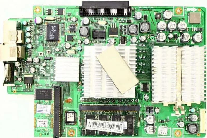
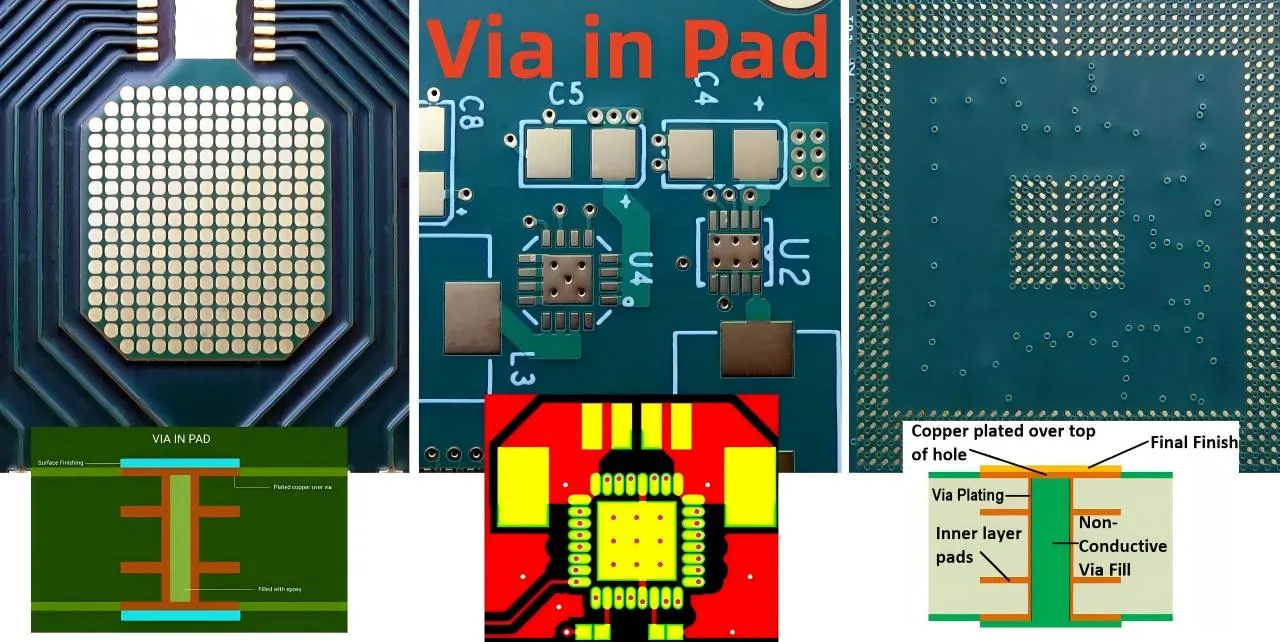
Via-in-pad (VIP) is a PCB design technique where a via—a small hole that connects different layers of a circuit board—is placed directly within the pad of a surface-mount component. Unlike traditional vias that are placed outside component pads, VIP allows for tighter layouts and shorter signal paths. This is especially useful in high-density designs where space is limited, such as in smartphones, wearables, and other compact electronics.
The primary benefit of via-in-pad is its ability to save space. By placing vias directly under components like ball grid arrays (BGAs), designers can reduce the overall footprint of the board. Additionally, it improves signal integrity by shortening trace lengths, which can minimize signal loss and interference. However, this technique comes with challenges, such as potential soldering issues and increased manufacturing complexity. Understanding via-in-pad design rules and best practices is crucial to avoid pitfalls and achieve reliable results.
Advantages and Disadvantages of Via-in-Pad
Before diving into the technical details, let's look at the pros and cons of using via-in-pad in your PCB designs. This will help you decide if it's the right choice for your project.
Advantages of Via-in-Pad
- Space Efficiency: Placing vias directly under component pads frees up valuable board space, allowing for more compact layouts. This is critical for designs with fine-pitch components like BGAs with pitches as small as 0.4mm.
- Improved Signal Integrity: Shorter trace lengths reduce parasitic inductance and capacitance, which can improve signal speeds and reduce noise. For high-speed designs operating at frequencies above 1 GHz, this can be a game-changer.
- Better Thermal Management: Vias under pads can help dissipate heat from components, especially in power-intensive applications, by providing a direct path to inner copper layers.
Disadvantages of Via-in-Pad
- Soldering Challenges: During assembly, solder can flow into the via, leading to insufficient solder on the pad and weak joints. This is often called "solder wicking."
- Increased Manufacturing Cost: VIP designs may require advanced fabrication techniques like via filling or plugging, which can raise production costs.
- Design Complexity: Implementing via-in-pad requires careful planning to meet manufacturing tolerances and ensure reliability.
Understanding these trade-offs will guide your decision on whether to use via-in-pad and how to approach its implementation.
Via-in-Pad Design Rules: Key Guidelines to Follow
To successfully integrate via-in-pad into your PCB layouts, you need to adhere to specific design rules. These guidelines ensure manufacturability, reliability, and performance. Below are the essential via-in-pad design rules to keep in mind.
1. Via Size and Pad Dimensions
The size of the via and its corresponding pad is critical. A via that's too large can cause solder wicking, while a via that's too small may not provide adequate electrical or thermal conductivity. As a general rule, the via diameter should be between 0.2mm and 0.3mm for most applications. The pad size should be at least 0.1mm to 0.15mm larger than the via diameter on all sides to ensure proper soldering.
2. Via Filling or Plugging
To prevent solder from flowing into the via during assembly, vias in pads are often filled or plugged. There are two common methods:
- Conductive Filling: Uses a conductive material like copper to fill the via, improving thermal and electrical conductivity.
- Non-Conductive Filling: Uses epoxy or resin to plug the via, preventing solder wicking while maintaining insulation.
Check with your PCB manufacturer to confirm their capabilities for via filling, as this process can impact costs and lead times.
3. Solder Mask and Tent Vias
For vias in pads that aren't filled, applying a solder mask over the via (tenting) can help reduce solder wicking. However, for high-density designs, filled vias are often preferred over tenting to ensure reliability.
4. Placement Under Fine-Pitch Components
For components with fine pitches (less than 0.5mm), such as BGAs, place vias symmetrically under the pads to maintain uniform soldering conditions. Avoid placing vias under the center of large components where heat dissipation might be uneven.
Via-in-Pad Best Practices for Optimal Results
Beyond the basic design rules, following via-in-pad best practices can elevate the quality of your PCB designs. These tips focus on balancing performance, manufacturability, and cost.
1. Collaborate with Your Manufacturer Early
Every PCB fabricator has specific capabilities and limitations when it comes to via-in-pad technology. Early collaboration ensures your design aligns with their processes, such as minimum via sizes or filling options. Provide detailed design files and discuss any VIP requirements upfront to avoid costly revisions.
2. Use Simulation Tools
Before finalizing your design, use simulation software to analyze signal integrity and thermal performance. For high-speed designs, ensure that the shorter trace lengths from via-in-pad don't introduce unexpected impedance mismatches. Typical impedance targets for high-speed signals are around 50 ohms for single-ended traces and 100 ohms for differential pairs.
3. Optimize Layer Stackup
In a multilayer PCB, plan your layer stackup to minimize signal interference near vias in pads. For instance, avoid routing high-speed signals on layers directly adjacent to power planes with VIPs to reduce noise coupling. A common 4-layer PCB stackup might have signal layers on top and bottom, with ground and power planes in the middle for shielding.
4. Test Prototypes Thoroughly
After fabrication, test your prototypes for soldering defects, thermal performance, and signal integrity. Use tools like X-ray inspection to check for voids or insufficient solder under components with vias in pads. This step helps identify issues before full-scale production.
Via-in-Pad Tutorial: A Step-by-Step Guide
Now that you understand the rules and best practices, let's walk through a via-in-pad step-by-step implementation in your PCB design process. This tutorial assumes you're using a standard PCB design tool and working on a high-density layout with a BGA component.
Step 1: Define Design Requirements
Start by identifying the components that require via-in-pad, such as a BGA with a 0.4mm pitch. Determine the number of vias needed based on signal, power, and ground connections. Review the component datasheet for pin assignments and spacing requirements.
Step 2: Set Via and Pad Parameters
In your PCB design software, set the via diameter to 0.25mm and the pad diameter to 0.4mm. Ensure the via drill size and finished hole size meet your manufacturer's specifications. If via filling is required, note this in your design documentation.
Step 3: Place Vias Under Pads
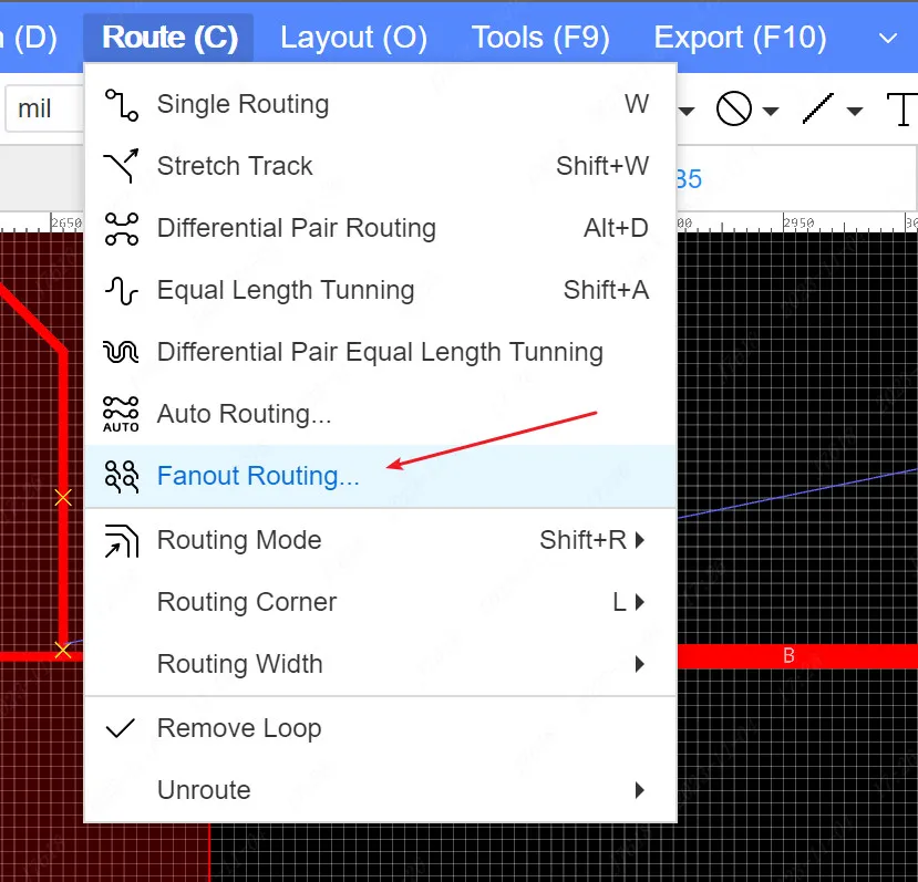
Place vias directly under the BGA pads, focusing on outer rows for signal escape routing. Use a fan-out pattern to route signals to inner layers while maintaining symmetry to avoid uneven stress during soldering. Keep at least 0.1mm clearance between adjacent vias to prevent manufacturing issues.
Step 4: Route Traces and Verify Clearances
Route traces from the vias to their respective layers, ensuring minimal length for high-speed signals. Check design rule constraints (DRC) in your software to verify that clearances and widths meet your design standards, such as a minimum trace width of 0.1mm for signals.
Step 5: Add Via Filling or Solder Mask
Specify via filling or tenting in your design notes. If using conductive filling, ensure the via material matches the thermal expansion properties of the board to avoid cracking. Update your Gerber files with these details for manufacturing.
Step 6: Review and Export Design
Run a final DRC and perform a visual inspection of the via-in-pad areas. Ensure all vias are properly aligned with pads and that no unintended overlaps occur. Export your design files, including a detailed bill of materials (BOM) and assembly notes for your manufacturer.
Common Mistakes to Avoid in Via-in-Pad Design
Even with the best intentions, mistakes can happen when implementing via-in-pad. Here are some common pitfalls and how to avoid them.
- Ignoring Manufacturer Guidelines: Failing to consult your fabricator can lead to unmanufacturable designs. Always confirm their via filling and drilling capabilities before finalizing your layout.
- Overlooking Solder Wicking: Without proper via filling or tenting, solder can flow into vias, causing weak joints. Plan for these protective measures during the design phase.
- Poor Thermal Planning: Placing too many vias under a component without considering heat dissipation can lead to hotspots. Use thermal vias strategically and simulate heat flow if possible.
Conclusion: Elevate Your PCB Designs with Via-in-Pad
Mastering via-in-pad technology can significantly enhance your PCB designs by saving space, improving signal integrity, and supporting high-density layouts. By following the via-in-pad design rules, adopting best practices, and using the step-by-step tutorial outlined in this guide, you can confidently integrate this technique into your projects. Remember to collaborate with your manufacturer, use simulation tools, and test prototypes to ensure success.