 ALLPCB


Choosing the right PCB design software for your IoT project can make or break your hardware development process. Whether you're working on low-power PCB design, small form factor PCB design, or integrating PCB antenna design software, the tool you select must align with the unique demands of IoT hardware design. In this guide, we'll walk you through the key factors to consider when picking the best software for IoT devices, ensuring your project is efficient, cost-effective, and scalable.
At ALLPCB, we understand the challenges of designing for the Internet of Things (IoT). That's why we've created this detailed resource to help you navigate the world of IoT hardware design tools. Below, we'll dive into the essential features to look for, specific considerations for IoT projects, and tips to optimize your design process.
Why PCB Design Software Matters for IoT Projects
IoT devices are at the heart of modern technology, connecting everything from smart home gadgets to industrial sensors. These devices often require compact designs, low power consumption, and seamless wireless communication. The right PCB design software ensures you can meet these needs by offering tools for precise layouts, power optimization, and antenna integration.
Without the proper software, you risk delays, costly redesigns, or performance issues. For instance, a poorly designed PCB for an IoT sensor might consume too much power, draining batteries in days instead of months. The software you choose must support the complexity of IoT systems while keeping the design process manageable.
Key Features to Look for in PCB Design Software for IoT Devices
When evaluating software for IoT hardware design, focus on features that address the specific challenges of these projects. Below are the critical elements to consider.
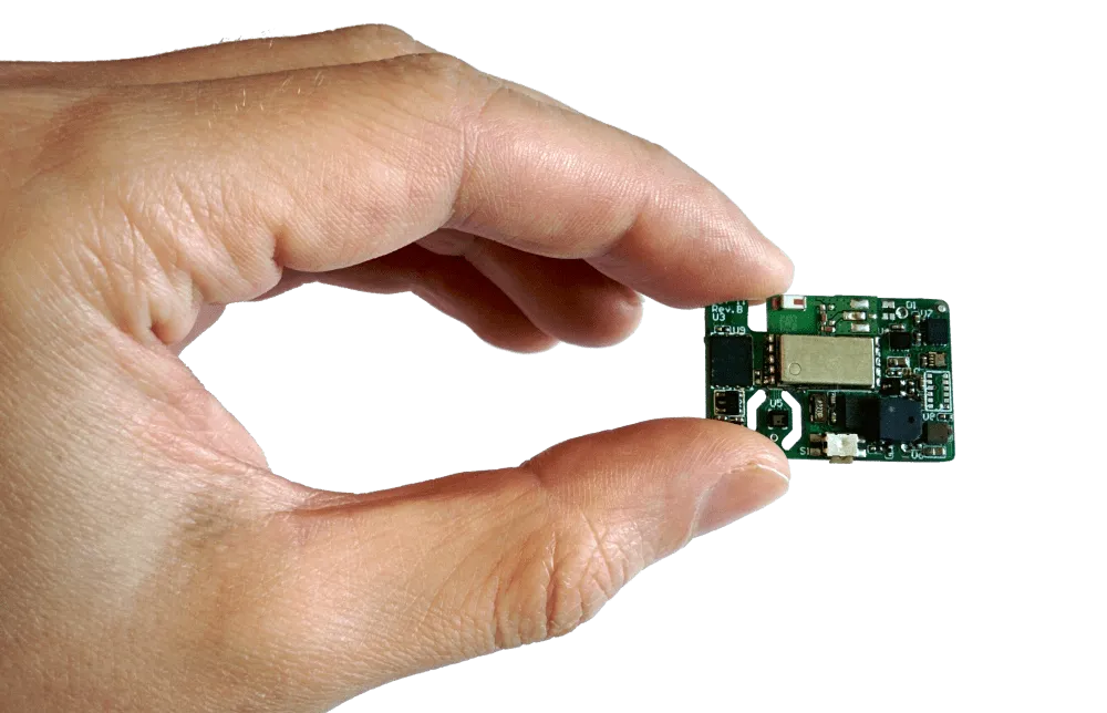
1. Support for Small Form Factor PCB Design
IoT devices are often tiny, requiring layouts that fit into tight spaces. Look for software that allows high-density component placement and multi-layer board design. This capability helps you pack more functionality into a smaller footprint, which is essential for wearables or embedded sensors.
For example, a smartwatch PCB might need to fit components into a space smaller than 2 square inches while maintaining signal integrity. Software with advanced routing tools can help you achieve this without compromising performance.
2. Tools for Low-Power PCB Design
Power efficiency is a cornerstone of IoT design, as many devices rely on batteries or energy harvesting. Choose software that offers power analysis tools to simulate and optimize energy consumption. Features like power integrity checks can help you identify and reduce leakage currents or inefficient routing that might drain power.
Consider a scenario where an IoT temperature sensor needs to operate for a year on a single coin cell battery. Software with power simulation can estimate consumption down to microamperes, helping you tweak the design for maximum efficiency.
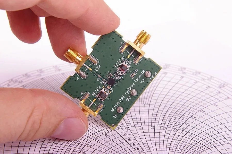
3. PCB Antenna Design Software Integration
Wireless connectivity is a defining feature of IoT devices, often requiring embedded antennas on the PCB. Not all design tools support antenna simulation or integration, so prioritize software with built-in or compatible modules for PCB antenna design. This ensures your antenna performs well within the 2.4 GHz or sub-6 GHz bands commonly used for IoT protocols like Wi-Fi or Bluetooth.
For instance, a meandered inverted-F antenna for a 2.4 GHz Wi-Fi module needs precise placement and tuning to avoid interference. Software with electromagnetic simulation can show surface current distribution, helping you fine-tune the design for optimal range and efficiency.
4. Compatibility with IoT Hardware Design Tools
IoT projects often involve integration with microcontrollers (MCUs), sensors, and communication modules. Your PCB design software should support libraries or integrations with popular IoT hardware platforms. This compatibility speeds up the design process by providing pre-built schematics or footprints for common components.
Imagine designing a smart home sensor with a specific MCU. Software with a robust component library can save hours by letting you drag and drop the MCU’s footprint instead of creating it from scratch.
5. Simulation and Testing Capabilities
Simulation tools are vital for catching issues before manufacturing. Look for software that offers signal integrity analysis, thermal simulation, and electromagnetic compatibility (EMC) testing. These features help ensure your IoT device operates reliably under real-world conditions.
For example, thermal simulation can predict if a power regulator on your PCB will overheat in a confined IoT enclosure. Addressing this in the design phase prevents costly hardware failures after production.
6. Scalability and Collaboration Features
IoT projects often evolve from prototypes to mass production. Choose software that supports scalability, allowing you to transition from a single board to thousands without redesigning. Additionally, look for collaboration tools if you’re working in a team. Cloud-based features or version control can streamline feedback and updates among engineers.
Special Considerations for IoT PCB Design
Beyond general features, IoT projects have unique challenges that influence software selection. Keep these factors in mind as you evaluate your options.
1. Miniaturization Challenges in Small Form Factor Design
Small form factor PCB design often means working with micro-vias and fine-pitch components. Your software must handle these elements with precision to avoid manufacturing errors. For instance, a 0.4mm pitch on a BGA package requires exact alignment, and the wrong tool might lead to misrouted traces or shorts.
2. Balancing Power and Performance in Low-Power PCB Design
Low-power PCB design isn’t just about minimizing consumption; it’s about balancing power with performance. Software should let you simulate different power modes (e.g., sleep vs. active) to ensure the device wakes up reliably while conserving energy. A tool that can model a sleep mode current of under 10 microamperes is invaluable for battery-powered IoT nodes.
3. Wireless Performance and PCB Antenna Design
Antenna design is critical for IoT connectivity, but it’s often overlooked. Poor antenna placement can result in a signal loss of 3 dB or more, halving your effective range. Software with antenna simulation can help you position the antenna away from noisy components and ground planes, ensuring stable communication.
4. Cost and Learning Curve
IoT projects often operate on tight budgets, especially for startups or small teams. Consider the cost of the software and whether it offers a free tier or trial for prototyping. Additionally, evaluate the learning curve. A tool with a steep learning curve might delay your project if your team isn’t experienced.
Steps to Evaluate and Choose the Right PCB Design Software
With so many options available, narrowing down the best software for your IoT project can feel overwhelming. Follow these steps to make an informed decision.
1. Define Your Project Requirements
Start by listing the specific needs of your IoT device. Does it require ultra-low power consumption? Is wireless range a priority? Will it fit into a tiny enclosure? Having a clear set of requirements helps you filter out tools that don’t meet your needs.
2. Research and Compare Features
Look at the features of different software packages, focusing on those relevant to IoT design. Create a comparison chart to weigh the pros and cons of each tool based on small form factor support, low-power tools, and antenna design capabilities.
3. Test with a Small Prototype
Many tools offer free trials or limited versions. Use these to design a simple IoT PCB, such as a basic sensor node, to see how the software handles your workflow. Pay attention to ease of use, simulation accuracy, and integration with manufacturing processes.
4. Check Community and Support Resources
A strong user community or detailed documentation can save you time when troubleshooting. Software with active forums, tutorials, or customer support ensures you’re not stuck when facing design challenges.
5. Partner with a Reliable Manufacturing Service
Once you’ve chosen your software, ensure it integrates smoothly with your manufacturing partner. At ALLPCB, we support a wide range of design file formats, making it easy to transition from design to production. Our team can also provide feedback on manufacturability to refine your PCB for IoT applications.
Common Pitfalls to Avoid When Choosing PCB Design Software
Selecting the wrong software can lead to wasted time and resources. Here are some pitfalls to watch out for.
1. Ignoring IoT-Specific Needs
General-purpose PCB tools might lack features for low-power or antenna design. Don’t settle for software that doesn’t address the unique demands of IoT hardware.
2. Overlooking Manufacturing Compatibility
Some software outputs files or designs that aren’t fully compatible with standard manufacturing processes. This can lead to errors or delays during production. Always verify that your tool aligns with industry standards.
3. Focusing Only on Cost
While budget is important, the cheapest option might lack critical features. Investing in a slightly more expensive tool with better simulation or scalability can save money in the long run by avoiding redesigns.
How ALLPCB Supports Your IoT PCB Design Journey
Designing an IoT PCB is only part of the journey; bringing it to life through manufacturing is equally important. At ALLPCB, we specialize in supporting IoT projects with fast, reliable PCB fabrication and assembly services. Whether you’re working on a small prototype or scaling to mass production, our team ensures your design translates perfectly to a finished product.
We also offer design-for-manufacturability (DFM) checks to catch potential issues early, saving you time and cost. With our expertise in small form factor and low-power designs, we’re your partner in creating cutting-edge IoT solutions.
Conclusion: Making the Right Choice for Your IoT Project
Selecting the right PCB design software for your IoT project is a critical decision that impacts every stage of development. By focusing on features like small form factor PCB design, low-power optimization, and PCB antenna design software, you can ensure your tool meets the demands of IoT hardware design. Follow a structured evaluation process, test your options, and avoid common pitfalls to find the perfect fit.
At ALLPCB, we’re committed to helping you succeed in your IoT endeavors. With the right software and a trusted manufacturing partner, you’re well on your way to creating innovative, connected devices that shape the future. Start exploring your options today, and let us support you in turning your designs into reality.


