ALLPCB


If you're an electrical engineer working on medical imaging systems, you might be wondering how to design a CT scanner PCB stackup that ensures high performance and reliability. In short, CT scanner PCBs require multilayer designs with high-density interconnects (HDI), controlled impedance, and a focus on signal integrity to handle the complex demands of medical imaging. This guide dives deep into the specifics of multilayer PCB design for medical imaging, covering everything from stackup strategies to signal integrity challenges. Let’s explore how to build robust PCBs for CT scanners that meet strict industry standards.
Introduction: Why CT Scanner PCB Design Matters
Computed Tomography (CT) scanners are critical tools in modern healthcare, producing detailed images of the human body to aid in diagnosis. At the heart of these machines are printed circuit boards (PCBs) that manage high-speed data acquisition, precise signal processing, and power distribution. Designing a PCB for a CT scanner isn’t just about connecting components; it’s about ensuring flawless performance under demanding conditions. From handling high-frequency signals to minimizing noise, every layer of the PCB stackup plays a vital role.
In this comprehensive guide, we’ll break down the essentials of CT scanner PCB stackup, multilayer PCB design for medical imaging, and key considerations like high-density interconnect (HDI) technology, controlled impedance PCB design, and signal integrity. Whether you’re optimizing an existing design or starting from scratch, this blog offers actionable insights to help you succeed.
Understanding CT Scanner PCB Stackup: The Foundation of Design
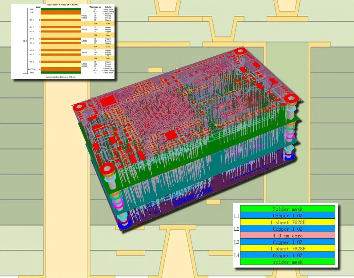
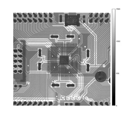
A PCB stackup refers to the arrangement of copper layers and insulating materials (dielectrics) in a multilayer board. For CT scanners, the stackup is critical because it determines how signals travel, how power is distributed, and how much noise or interference the board can handle. A typical CT scanner PCB might have 8 to 16 layers, depending on the complexity of the system.
Why so many layers? CT scanners process massive amounts of data from X-ray detectors at high speeds. This requires separate layers for signal routing, power delivery, and grounding to minimize crosstalk and electromagnetic interference (EMI). A well-designed stackup ensures that high-speed signals—often running at frequencies above 100 MHz—maintain their integrity while avoiding delays or distortions.
For example, a common stackup for a CT scanner PCB might include:
- Top Layer: Signal routing for high-speed data lines.
- Ground Plane: Directly below to shield signals and reduce noise.
- Power Plane: For stable voltage distribution, often at 3.3V or 5V for digital components.
- Inner Signal Layers: For additional routing of analog and digital signals.
- Bottom Layer: Additional grounding or low-speed signals.
Engineers must also consider the dielectric material between layers. Materials like FR-4 are common for cost-effective designs, but high-performance CT scanner PCBs might use advanced materials like Rogers or Isola for better signal performance at high frequencies.
Multilayer PCB Design for Medical Imaging: Key Principles
Designing a multilayer PCB for medical imaging systems like CT scanners involves balancing several factors: space constraints, signal speed, and regulatory compliance. Let’s explore the core principles that guide this process.
1. Layer Planning for Functionality
Each layer in a multilayer PCB serves a specific purpose. For CT scanners, you’ll often dedicate layers to high-speed digital signals (like data from X-ray detectors), analog signals (for sensor inputs), and power distribution. A typical 12-layer board might allocate 4 layers for signals, 4 for ground planes, and 4 for power planes to ensure isolation and stability.
2. Minimizing Crosstalk and EMI
Crosstalk occurs when signals on adjacent traces interfere with each other, a common issue in densely packed CT scanner PCBs. To combat this, engineers place ground planes between signal layers to act as shields. Additionally, maintaining a minimum spacing between traces—often 5 to 10 mils for high-speed lines—reduces unwanted coupling.
3. Compliance with Medical Standards
Medical devices must meet strict standards like IEC 60601-1 for electrical safety and electromagnetic compatibility (EMC). Your PCB design must minimize EMI to avoid interfering with other medical equipment. This often means using continuous ground planes and proper shielding techniques.
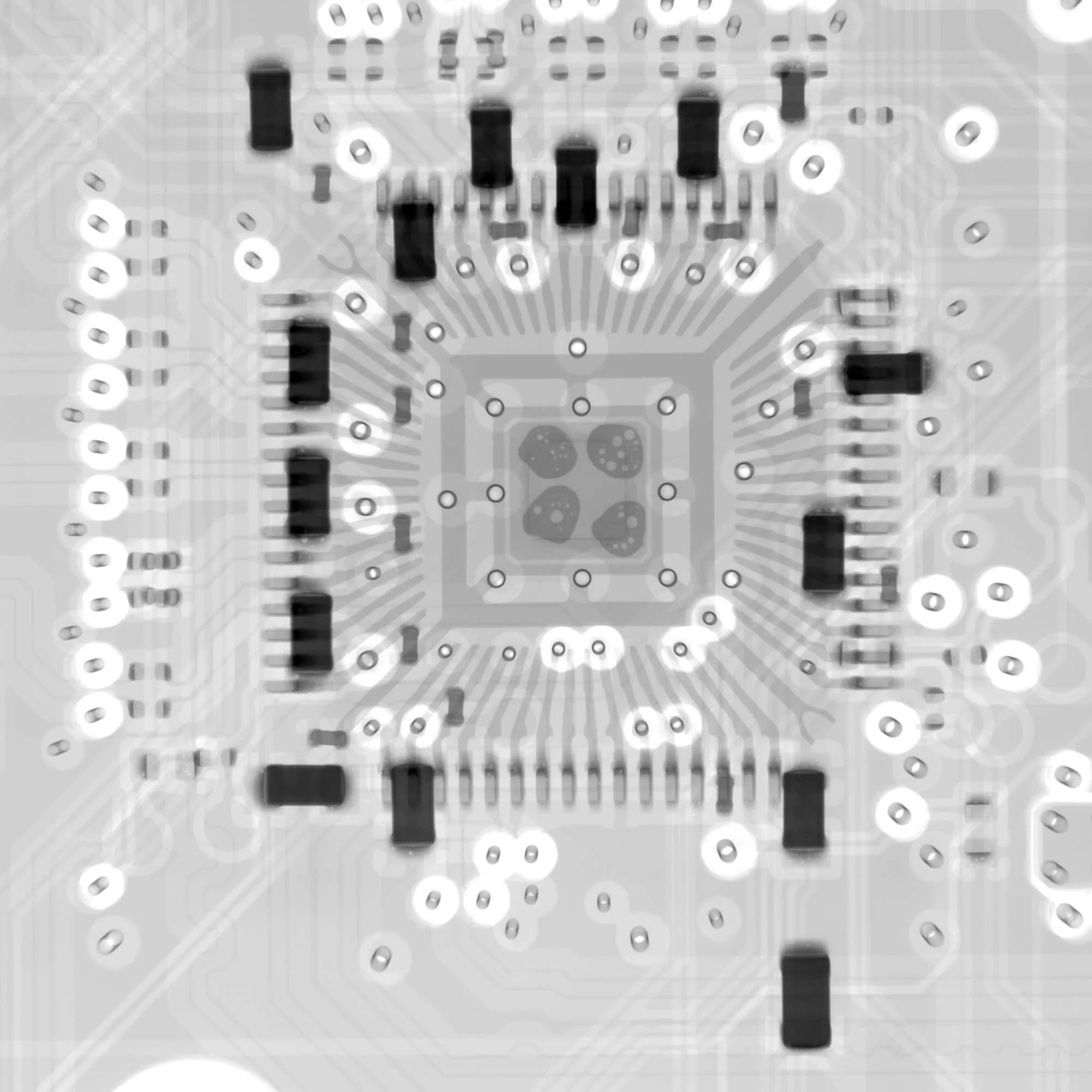
High-Density Interconnect (HDI) PCB in CT Scanners
CT scanner PCBs often require high-density interconnect (HDI) technology to fit more components and connections into a smaller space. HDI PCBs use microvias (tiny holes less than 6 mils in diameter) and fine-pitch traces (often below 3 mils) to achieve this. Why is HDI crucial for medical imaging?
First, CT scanners have hundreds or even thousands of connections between detectors, processors, and memory units. HDI allows engineers to route these connections efficiently without increasing the board size. Second, HDI supports smaller components like ball grid arrays (BGAs), which are common in high-performance processors used for image reconstruction.
However, HDI design comes with challenges. The smaller vias and traces are more prone to manufacturing defects, so you’ll need to work closely with your PCB fabricator to ensure precision. Additionally, HDI boards are more expensive, so cost-benefit analysis is essential for your project.
For instance, an HDI PCB for a CT scanner might use a 1+N+1 structure, where “N” represents the number of core layers, and the “1”s are build-up layers with microvias on each side. This setup allows for dense routing while maintaining signal integrity.
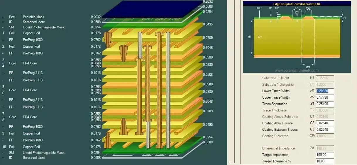
Controlled Impedance PCB Design: Ensuring Signal Accuracy
Controlled impedance is a cornerstone of CT scanner PCB design. Impedance refers to the resistance a signal encounters as it travels along a trace. If the impedance isn’t consistent, signals can reflect back, causing data loss or distortion—a disaster for medical imaging where accuracy is non-negotiable.
In CT scanners, high-speed signals often require a characteristic impedance of 50 ohms for single-ended traces or 100 ohms for differential pairs. Achieving this involves careful design of trace width, spacing, and dielectric thickness. For example, on a standard FR-4 board, a 50-ohm trace might be 6 mils wide with a 1.6 mm board thickness.
To implement controlled impedance, use simulation tools like Altium Designer or Cadence to model your PCB stackup before fabrication. These tools can predict impedance values based on your layer arrangement and material choices. After manufacturing, test the board with a time-domain reflectometer (TDR) to verify that impedance matches your design specs.
Challenges arise when dealing with mixed-signal designs, common in CT scanners. Analog signals from detectors might require different impedance values than digital signals for data processing. In such cases, segment your board into zones with tailored stackups for each signal type.
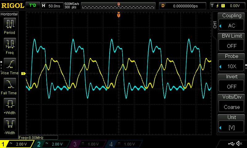
Signal Integrity in CT Scanner PCBs: Avoiding Data Loss
Signal integrity refers to the quality of electrical signals as they travel through a PCB. Poor signal integrity can lead to data errors, which in a CT scanner could mean inaccurate images or missed diagnoses. Given that CT scanners handle signals at speeds exceeding 1 Gbps, maintaining signal integrity is a top priority.
Key Factors Affecting Signal Integrity
Several factors can degrade signal integrity in CT scanner PCBs:
- Reflections: Caused by impedance mismatches, leading to signal echoes. Use controlled impedance designs to minimize this.
- Crosstalk: Interference between nearby traces. Increase trace spacing or add ground planes to reduce it.
- Signal Attenuation: Loss of signal strength over long traces, especially at high frequencies. Use shorter traces or low-loss dielectric materials.
- Noise: External or internal EMI can corrupt signals. Proper grounding and shielding are essential.
Practical Tips for Signal Integrity
Here are actionable steps to ensure signal integrity in your CT scanner PCB design:
- Use Differential Signaling: For high-speed data, differential pairs (like those used in USB or PCIe) reduce noise by canceling out common-mode interference.
- Route Critical Signals First: Prioritize high-speed lines during layout to give them the shortest, straightest paths.
- Add Decoupling Capacitors: Place capacitors near power pins of ICs to filter noise. A 0.1 μF capacitor is often sufficient for most digital components.
- Simulate Your Design: Use tools like HyperLynx to simulate signal behavior and identify potential issues before manufacturing.
For example, in a recent project, a team designing a CT scanner PCB noticed signal degradation at 500 MHz due to long trace lengths. By shortening the traces and switching to a low-loss dielectric material, they reduced attenuation by 20%, ensuring clear image data transmission.
Challenges and Solutions in CT Scanner PCB Design
Designing PCBs for CT scanners isn’t without hurdles. Here are some common challenges and how to address them:
- Heat Dissipation: High-power components generate heat, which can affect performance. Use thermal vias and copper pours to dissipate heat, and consider materials with high thermal conductivity.
- Component Density: Fitting numerous components into a small space increases the risk of interference. HDI technology and careful component placement can help.
- Cost Constraints: Advanced materials and HDI designs are expensive. Balance performance needs with budget by prioritizing critical areas for high-end solutions.
Conclusion: Building Better CT Scanner PCBs
Designing a PCB for a CT scanner is a complex but rewarding task. By focusing on a well-planned CT scanner PCB stackup, leveraging multilayer PCB design for medical imaging, incorporating high-density interconnect technology, ensuring controlled impedance, and prioritizing signal integrity, you can create boards that meet the rigorous demands of medical imaging.
Remember to simulate your designs, collaborate with fabricators, and test rigorously to catch issues early. With these strategies, you’ll be well-equipped to tackle the challenges of CT scanner PCB design and contribute to life-saving technology.
Have you worked on a CT scanner PCB project? Share your experiences or questions in the comments below—we’d love to hear from you! For more insights on PCB design, subscribe to our blog or reach out for personalized guidance.