 ALLPCB


Designing a double-layer printed circuit board (PCB) is a balancing act between functionality, performance, and cost. For engineers, creating a reliable and efficient PCB without inflating production expenses is critical, especially for small-scale projects or prototypes. Double-layer PCBs, with conductive layers on both sides of the substrate, offer more routing flexibility than single-layer boards while remaining more affordable than multilayer designs. However, poor design choices can quickly escalate costs, from material waste to manufacturing complexities.
In this blog, we share practical, actionable tips to help engineers optimize double-layer PCB designs for cost-effectiveness without compromising quality. Drawing from industry best practices and technical insights, we'll cover strategies to streamline your design process, reduce fabrication expenses, and ensure your PCB performs reliably. Whether you're a seasoned designer or tackling your first double-layer board, these tips will guide you toward smarter, budget-friendly decisions.
Why Cost-Effective Double-Layer PCB Design Matters
Double-layer PCBs are widely used in consumer electronics, automotive systems, and industrial applications due to their versatility and affordability. According to industry data, double-layer PCBs account for approximately 40% of the global PCB market, valued at over $80 billion in 2023. However, fabrication costs can vary significantly based on design complexity, material choices, and manufacturing requirements. By optimizing your design, you can reduce costs by up to 30% without sacrificing performance, making your project more competitive in the market.
Cost overruns often stem from inefficient layouts, non-standard specifications, or over-engineering. For example, specifying unnecessarily tight tolerances or complex features like microvias can increase fabrication costs by 20-50%. Our goal is to help you avoid these pitfalls and create designs that are both economical and reliable.
Tip 1: Optimize Board Size and Shape
The physical dimensions and shape of your PCB directly impact material and fabrication costs. Larger boards require more raw materials, such as FR4 (the most common substrate), which can account for 20-30% of total production costs. Non-standard shapes, like circular or irregular outlines, often incur additional tooling charges due to specialized cutting processes.
Actionable Advice:
-
Minimize Board Size: Design the smallest board possible while maintaining functionality. For example, a 10% reduction in board area can save 5-10% on material costs.
-
Use Standard Shapes: Stick to rectangular or square boards to avoid extra milling fees, which can add $10-50 per board for non-standard shapes.
-
Panelize Efficiently: Arrange multiple PCBs on a single panel to maximize material usage. For instance, fitting 10 boards on a panel instead of 8 can reduce per-unit costs by 20%.
Example: For a recent IoT sensor project, we reduced the PCB size from 50x50 mm to 40x40 mm by optimizing component placement, saving 15% on material costs without affecting performance.
Tip 2: Simplify Component Placement
Component placement affects both assembly costs and signal integrity. Dense or poorly organized layouts can increase assembly time and require expensive automated equipment. Proper placement also minimizes trace lengths, reducing signal delays and potential crosstalk.
Actionable Advice:
-
Group Similar Components: Place components with similar functions (e.g., power management ICs) close together to shorten trace lengths. This can reduce routing time by 10-20%.
-
Maintain Uniform Orientation: Orient components in the same direction (0° or 90°) to simplify pick-and-place machine programming, potentially lowering assembly costs by 5-10%.
-
Ensure Adequate Spacing: Leave at least 100 mils (2.54 mm) between components and 100 mils from the board edge to avoid manufacturing defects. For high-density designs, consult your fabricator's design rules.
Tip 3: Streamline Trace Routing
Efficient trace routing reduces material usage and improves signal integrity. Double-layer PCBs rely heavily on top and bottom layers for routing, as they lack the additional planes of multilayer boards. Overly complex routing can increase copper usage and fabrication time.
Actionable Advice:
-
Use Wider Traces When Possible: Standard trace widths of 8-10 mils (0.2-0.25 mm) are cost-effective for most signals carrying 10-20 mA. Narrower traces (e.g., 4 mils) require higher precision and can increase costs by 10-15%.
-
Minimize Vias: Each via adds drilling and plating costs. Reducing via count by 20% can save 5-10% on fabrication. Use single vias to connect top and bottom layers instead of multiple redundant vias.
-
Route Orthogonally: Route traces horizontally on one layer and vertically on the other to reduce crosstalk. For example, a 10 GHz signal on a 5-mil trace requires 10-mil spacing to maintain 50Ω impedance.
Example: In a recent audio amplifier design, we reduced via count from 150 to 100 by optimizing trace paths, saving 8% on fabrication costs while maintaining signal quality.
Tip 4: Choose Cost-Effective Materials
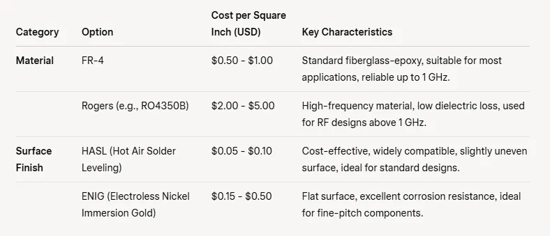
Material selection is a major cost driver. FR-4, a fiberglass-epoxy laminate, is the default choice for double-layer PCBs due to its low cost ($0.50-$1.00 per square inch) and reliability. Exotic materials like Rogers or polyimide can double or triple costs.
Actionable Advice:
-
Stick to Standard FR-4: Unless your design requires high-frequency performance (>1 GHz) or extreme thermal resistance (>150°C), FR-4 with a 1 oz copper weight is sufficient.
-
Avoid Premium Finishes: Use HASL (Hot Air Solder Leveling) instead of ENIG (Electroless Nickel Immersion Gold) for surface finishes to save $0.10-$0.50 per square inch.
-
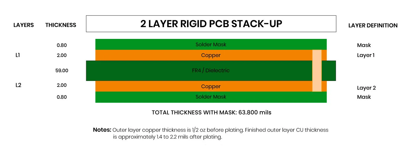
Specify Standard Thickness: Use 1.6 mm board thickness, the industry standard, to avoid custom lamination fees, which can add 10% to costs.
Tip 5: Leverage Design Rule Checks (DRC)
Design Rule Checks (DRC) in PCB design software like KiCad or Altium Designer catch errors early, preventing costly revisions. Running DRC throughout the design process ensures compliance with your fabricator's capabilities.
Actionable Advice:
-
Run DRC Frequently: Check your design after each major step (e.g., component placement, routing) to catch issues like insufficient trace spacing or unconnected nets.
-
Use Fabricator's Rules: Import your manufacturer's DRC settings to align with their minimum tolerances (e.g., 6-mil trace width, 8-mil drill size).
-
Validate Gerber Files: Use a Gerber viewer to confirm your output files match the design intent, avoiding production delays.
Example: A client avoided a $500 rework fee by catching a 5-mil trace spacing error during DRC, which violated the fabricator's 6-mil minimum.
Tip 6: Plan for Assembly and Testing
Assembly and testing costs can rival fabrication expenses, especially for low-volume runs. Hand assembly is viable for prototypes, but automated assembly is more cost-effective for runs exceeding 100 units.
Actionable Advice:
-
Use Surface Mount Technology (SMT): SMT components are cheaper to assemble than through-hole parts, reducing labor costs by 20-30%. For example, a 0805 resistor costs $0.01 vs. $0.05 for a through-hole equivalent.
-
Include Test Points: Add test points for critical nets (e.g., power, ground) to simplify in-circuit testing, reducing debugging time by 15-25%.
-
Optimize BOM: Use standard, widely available components to avoid supply chain delays and premium pricing. A common 1 kΩ resistor might cost $0.02, while a specialty part could be $0.50.
Tip 7: Collaborate with Your Manufacturer
Early collaboration with your PCB manufacturer can prevent costly design iterations. Fabricators often provide free Design for Manufacturability (DFM) checks to identify issues like insufficient annular rings or non-standard hole sizes.
Actionable Advice:
-
Request DFM Feedback: Submit your design for a pre-production review to catch manufacturability issues, potentially saving 10-20% on rework costs.
-
Ask About Standard Specs: Use your fabricator's standard stack-up (e.g., 1.6 mm FR-4, 1 oz copper) to avoid custom setup fees.
-
Negotiate Volume Discounts: For runs over 500 units, negotiate bulk pricing, which can reduce per-unit costs by 15-25%.
How ALLPCB Supports Cost-Effective PCB Design
At ALLPCB, we understand the importance of balancing cost and quality in double-layer PCB design. Our quick-turn prototyping services deliver boards in as little as 24 hours, allowing engineers to test and refine designs rapidly, minimizing costly revisions. With global logistics and advanced manufacturing facilities, we offer competitive pricing, starting at $0.50 per square inch for standard double-layer PCBs. Our free DFM analysis ensures your design aligns with our state-of-the-art equipment, reducing production errors and saving you up to 20% on fabrication costs. Whether you're prototyping or scaling to production, ALLPCB's expertise and resources help you achieve cost-effective, high-quality results.
Conclusion: Design Smarter, Save More
Cost-effective double-layer PCB design is about making informed choices at every stage, from layout to material selection. By optimizing board size, simplifying routing, choosing standard materials, and collaborating with your manufacturer, you can reduce costs by 20-30% while maintaining performance. Tools like DRC and DFM checks further ensure your design is production-ready, saving time and money.
Start applying these tips to your next project, and you'll see the difference in both your budget and your board's reliability. For engineers looking to streamline their workflow, partnering with a trusted manufacturer like ALLPCB can make cost-effective design even easier.


