ALLPCB


In the world of printed circuit board (PCB) design, shape matters more than ever. While rectangular PCBs have long been the standard, modern electronics often demand non-rectangular PCB design to fit unique product enclosures or optimize performance. But how do complex PCB shapes impact PCB shape signal integrity? Can high-speed PCB routing in irregular shapes maintain performance? And what about impedance control in complex PCB shapes? In this blog, we’ll dive deep into these topics, offering practical insights and actionable tips to help engineers master signal integrity in non-traditional PCB designs.
Why Complex PCB Shapes Are Becoming the Norm
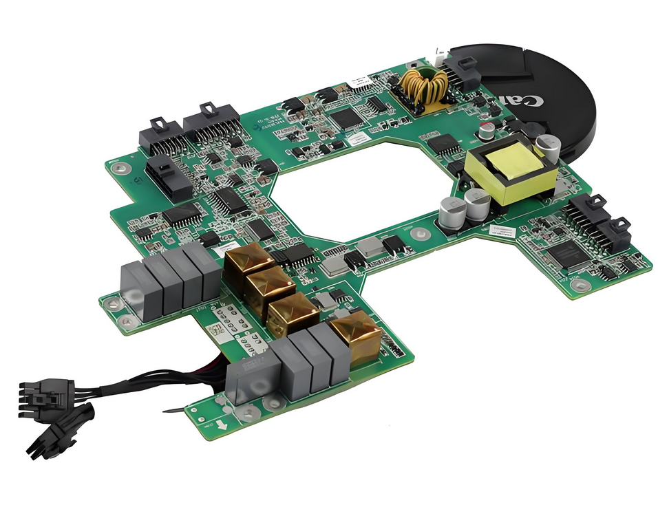
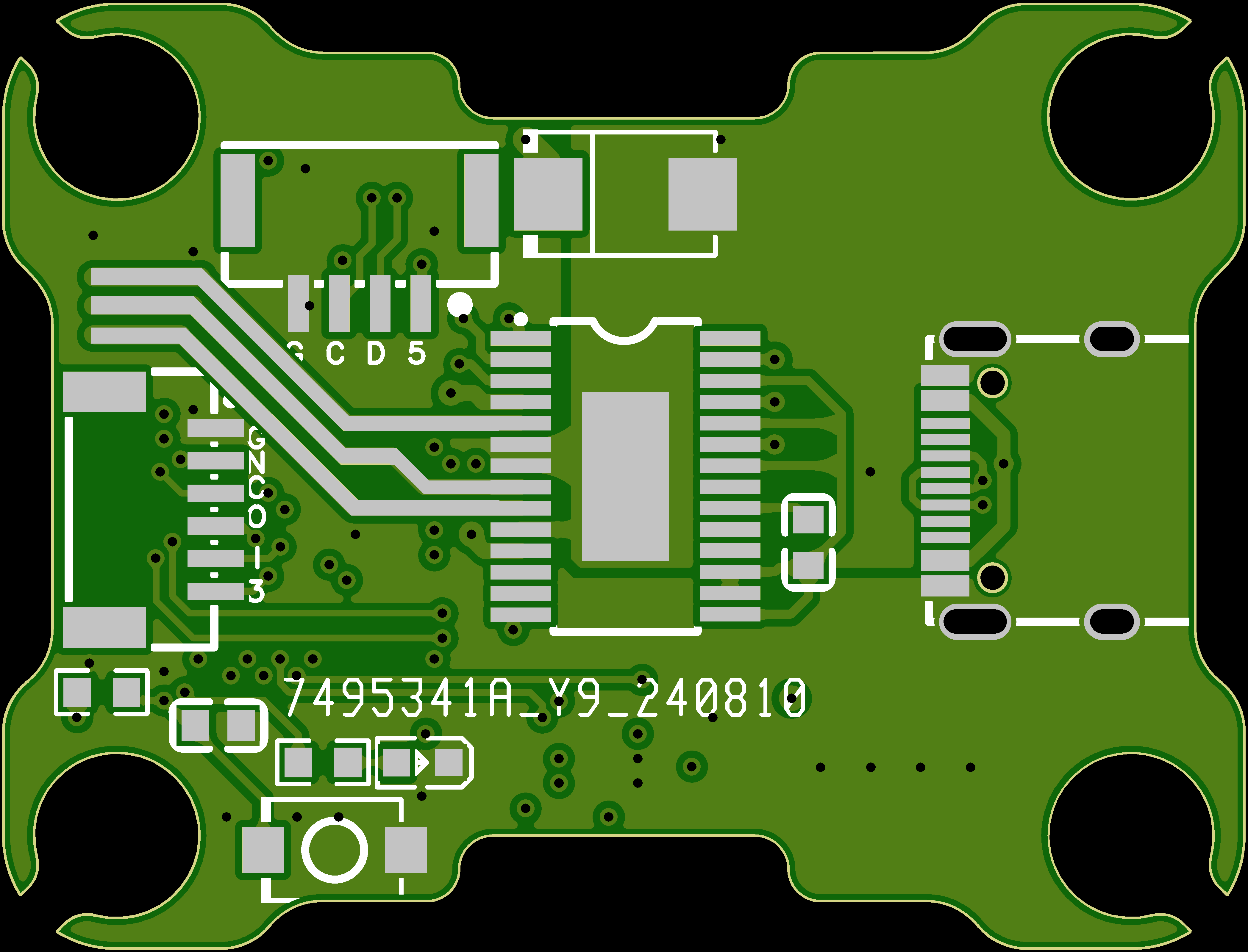
As devices become smaller, sleeker, and more specialized, the need for custom-shaped PCBs grows. Think about wearable technology, automotive sensors, or IoT devices—many of these products don’t fit neatly into a rectangular form factor. Non-rectangular designs allow PCBs to conform to curved surfaces, fit into tight spaces, or align with aesthetic product designs.
However, moving beyond rectangles introduces challenges for signal integrity, especially in high-speed applications. Signal paths may become uneven, impedance can fluctuate, and electromagnetic interference (EMI) risks increase. Understanding how to address these issues is critical for engineers working on cutting-edge designs.
Understanding PCB Shape and Signal Integrity
Signal integrity refers to the quality of an electrical signal as it travels through a PCB. In high-speed designs, even small disruptions can cause data errors, timing issues, or complete system failures. When it comes to PCB shape signal integrity, non-rectangular designs can complicate things in several ways:
- Irregular Trace Lengths: Non-rectangular shapes often lead to uneven trace routing, which can cause signal delays or mismatches in differential pairs.
- Impedance Variations: Changes in board shape can affect the dielectric properties around traces, leading to impedance mismatches.
- EMI Risks: Complex shapes may create areas where signals are more prone to interference or crosstalk due to tighter spacing or unusual ground plane configurations.
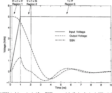
For high-speed designs operating at frequencies above 1 GHz, these factors become even more critical. A signal traveling at such speeds can degrade if impedance varies by even a few ohms, typically requiring a controlled impedance of 50 ohms for single-ended traces or 100 ohms for differential pairs.
Challenges of Non-Rectangular PCB Design
Designing a non-rectangular PCB introduces unique hurdles that directly impact performance. Let’s break down some of the key challenges:
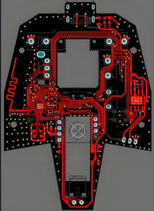
1. Routing in Tight or Irregular Spaces
In a rectangular PCB, traces often follow straight, predictable paths. But with high-speed PCB routing in irregular shapes, engineers must navigate curves, angles, and confined areas. This can lead to longer trace lengths or sharp bends, both of which degrade signal quality. For instance, a 90-degree bend in a trace can cause signal reflection, increasing noise by up to 10% in some high-speed scenarios.
2. Ground Plane Disruptions
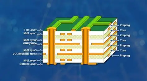
A solid, uninterrupted ground plane is essential for maintaining signal integrity. In non-rectangular designs, the ground plane may need to conform to the board’s shape, creating gaps or splits. These disruptions can force return currents to take longer paths, increasing loop inductance and EMI risks.
3. Impedance Control in Complex PCB Shapes
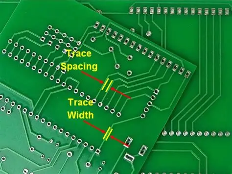
Achieving impedance control in complex PCB shapes is a significant challenge. Impedance depends on trace width, spacing, and the dielectric constant of the substrate material. In irregular shapes, maintaining consistent trace geometry becomes difficult, often leading to impedance variations. For example, a trace narrowing to fit a curved edge might see its impedance rise from 50 ohms to 60 ohms, causing signal reflections.
Strategies for Mastering Signal Integrity in Complex PCB Shapes
Despite the challenges, it’s possible to achieve excellent signal integrity in non-rectangular PCB designs. Here are proven strategies to guide your approach:
1. Optimize Trace Routing for High-Speed Signals
For high-speed PCB routing in irregular shapes, prioritize smooth, gradual bends over sharp angles. A 45-degree bend or a curved trace reduces signal reflection compared to a 90-degree turn. Additionally, use length matching for differential pairs to ensure signals arrive at the same time, avoiding skew. Modern design software can calculate and adjust trace lengths to within 0.1 mm accuracy for signals operating at 5 Gbps or higher.
2. Maintain Consistent Impedance
To achieve impedance control in complex PCB shapes, carefully design trace widths and spacing based on the board material’s dielectric constant (Dk). For instance, a standard FR-4 material with a Dk of 4.5 might require a trace width of 0.2 mm for a 50-ohm impedance on a microstrip line. Use simulation tools to model impedance across the board, especially in areas where the shape changes. If narrowing traces is unavoidable, compensate by adjusting the dielectric thickness or adding vias to stabilize impedance.
3. Design Robust Ground Planes
Even in non-rectangular designs, strive for a continuous ground plane beneath high-speed signals. If splits are necessary due to the board’s shape, place stitching vias to provide a low-inductance return path. Aim for via spacing of less than 1/20th of the signal’s wavelength to minimize EMI. For a 2.4 GHz signal, this translates to vias spaced less than 6 mm apart.
4. Use Advanced Materials
Consider using low-loss materials with a stable dielectric constant for complex shapes. Materials with a Dk variation of less than 0.1 across the board can help maintain consistent impedance. While these materials may cost 20-30% more than standard options, they significantly reduce signal loss in high-speed applications above 10 Gbps.
5. Simulate and Test Early
Simulation is your best friend when working with non-rectangular designs. Use electromagnetic field solvers to predict signal behavior and identify potential issues like crosstalk or impedance mismatches. After fabrication, perform time-domain reflectometry (TDR) testing to verify impedance values, aiming for variations of less than ±5% from the target (e.g., 50 ohms ±2.5 ohms).
Tools and Technologies for Non-Rectangular PCB Design
Designing complex PCB shapes requires the right tools to ensure precision and performance. Here are some key technologies to leverage:
- Advanced EDA Software: Use electronic design automation (EDA) tools with built-in signal integrity analysis to model and optimize non-rectangular layouts. These tools can simulate signal propagation at speeds up to 25 Gbps and beyond.
- 3D Modeling: 3D design capabilities allow you to visualize how a non-rectangular PCB fits into the final product, ensuring that shape constraints don’t compromise routing or component placement.
- Automated Impedance Calculators: Many design platforms offer calculators to determine trace dimensions for specific impedance values, saving time and reducing errors in complex layouts.
Real-World Applications of Non-Rectangular PCBs
Non-rectangular PCBs are already making a big impact in various industries. Here are a few examples:
- Wearables: Circular or flexible PCBs in smartwatches and fitness trackers conform to curved designs while maintaining signal integrity for wireless communication at 2.4 GHz.
- Automotive: Irregular-shaped PCBs in sensors and control units fit into compact, non-standard spaces, supporting high-speed data transfer for systems like adaptive cruise control.
- Medical Devices: Custom-shaped PCBs in implantable devices optimize space and ensure reliable signal transmission for critical health monitoring functions.
Best Practices for Fabrication and Assembly
Once your design is ready, fabrication and assembly present their own challenges for non-rectangular PCBs. Keep these tips in mind:
- Communicate with Fabricators: Provide detailed documentation on shape requirements and impedance targets to avoid manufacturing errors. Specify tolerances for trace widths (e.g., ±0.025 mm) to ensure consistency.
- Panelization: Non-rectangular PCBs may require custom panelization to maximize yield during production. Work with your manufacturer to balance cost and efficiency.
- Testing: Request in-circuit testing (ICT) and functional testing post-assembly to verify signal integrity, especially for high-speed signals above 1 GHz.
Future Trends in Complex PCB Shapes and Signal Integrity
The demand for non-rectangular PCBs will only grow as devices become more compact and specialized. Emerging trends include:
- Flexible and Rigid-Flex PCBs: These allow even more complex shapes while maintaining signal integrity through advanced materials and design techniques.
- AI-Driven Design: Artificial intelligence is being integrated into EDA tools to optimize routing and impedance control automatically, even in irregular shapes.
- Higher Frequencies: As 5G and beyond become mainstream, PCBs will need to handle frequencies up to 100 GHz, placing greater emphasis on shape and material selection for signal integrity.
Conclusion: Shaping the Future of PCB Design
Mastering PCB shape signal integrity in non-rectangular designs is no small feat, but with the right strategies, tools, and mindset, it’s entirely achievable. By focusing on optimized routing, consistent impedance, and robust ground planes, engineers can tackle the challenges of non-rectangular PCB design and ensure reliable performance in high-speed applications. Whether you’re working on wearables, automotive systems, or medical devices, embracing high-speed PCB routing in irregular shapes and impedance control in complex PCB shapes opens up new possibilities for innovation.